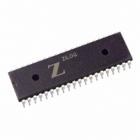
Z0847006PSG Zilog, Z0847006PSG Datasheet - Page 110

Z0847006PSG
Manufacturer Part Number
Z0847006PSG
Description
IC 6MHZ Z80 NMOS DART 40-DIP
Manufacturer
Zilog
Series
Z80r
Datasheet
1.Z0847006PSG.pdf
(330 pages)
Specifications of Z0847006PSG
Processor Type
Z80
Features
Dual Channel Asynchronous Receiver/Transmitter (DART)
Speed
6MHz
Voltage
5V
Mounting Type
Through Hole
Package / Case
40-DIP (0.620", 15.75mm)
Mounting Style
Through Hole
Cpu Speed
6MHz
Digital Ic Case Style
DIP
No. Of Pins
40
Supply Voltage Range
5V
Operating Temperature Range
0°C To +70°C
Svhc
No SVHC (18-Jun-2010)
Base Number
847006
Rohs Compliant
Yes
Clock Frequency
6MHz
Lead Free Status / RoHS Status
Lead free / RoHS Compliant
Available stocks
Company
Part Number
Manufacturer
Quantity
Price
Company:
Part Number:
Z0847006PSG
Manufacturer:
Zilog
Quantity:
22
- Current page: 110 of 330
- Download datasheet (3Mb)
UM008101-0601
< % 2 7 2 G T K R J G T C N U
7 U G T / C P W C N
Write Registers
Control bytes must be written to all relevant registers in the DMA at power-
up initialization. This section describes and illustrates each of the write
registers, WR0 through WR6, to which control bytes can be written. The
convention of calling the control bytes written to WR6 “commands” is
often used, because they are commonly used within CPU interrupt service
routines and at other times during system operation in addition to their use
at power-up initialization of the DMA.
“Internal Structure” on page 71 gives an organizational overview of the
write registers (Figure 30) and describes the access method. Control bytes
are written to one or more of the write register groups (WR6-WR0) by first
writing a byte to the “base register” in that group. All groups have base
registers and most groups have additional associated registers. The asso-
ciated registers in a group are sequentially accessed by first writing a byte
to the base register. The base register byte contains both control bits for
DMA function control, and pointer bits (1s) to one or more of the asso-
ciated registers in the base register’s group.
Figure 39 for WR0 illustrates this. In this figure, the sequence in which
associated registers within a group can be written to is shown by the
vertical position of the associated registers. For example, if a byte written to
the DMA contains the bits that identify WR0 (bits D0, D1, and D7), and
also contains 1s in the bit positions that point to associated registers 2 and 4,
then the next two bytes written to the DMA after the base register byte is
stored in these two associated registers, in that order.
Figure 40 through Figure 46 illustrate and describe each of seven base
registers and their associated registers. These figures, unlike Figure 30, do
not include the 16-bit counters associated with the starting-address and
block-length registers.
Direct Memory Access
Related parts for Z0847006PSG
Image
Part Number
Description
Manufacturer
Datasheet
Request
R

Part Number:
Description:
Customer Procurement Spec(CPS)
Manufacturer:
ZILOG [Zilog, Inc.]
Datasheet:

Part Number:
Description:
Communication Controllers, ZILOG INTELLIGENT PERIPHERAL CONTROLLER (ZIP)
Manufacturer:
Zilog, Inc.
Datasheet:

Part Number:
Description:
KIT DEV FOR Z8 ENCORE 16K TO 64K
Manufacturer:
Zilog
Datasheet:

Part Number:
Description:
KIT DEV Z8 ENCORE XP 28-PIN
Manufacturer:
Zilog
Datasheet:

Part Number:
Description:
DEV KIT FOR Z8 ENCORE 8K/4K
Manufacturer:
Zilog
Datasheet:

Part Number:
Description:
KIT DEV Z8 ENCORE XP 28-PIN
Manufacturer:
Zilog
Datasheet:

Part Number:
Description:
DEV KIT FOR Z8 ENCORE 4K TO 8K
Manufacturer:
Zilog
Datasheet:

Part Number:
Description:
CMOS Z8 microcontroller. ROM 16 Kbytes, RAM 256 bytes, speed 16 MHz, 32 lines I/O, 3.0V to 5.5V
Manufacturer:
Zilog, Inc.
Datasheet:

Part Number:
Description:
Low-cost microcontroller. 512 bytes ROM, 61 bytes RAM, 8 MHz
Manufacturer:
Zilog, Inc.
Datasheet:

Part Number:
Description:
Z8 4K OTP Microcontroller
Manufacturer:
Zilog, Inc.
Datasheet:

Part Number:
Description:
CMOS SUPER8 ROMLESS MCU
Manufacturer:
Zilog, Inc.
Datasheet:

Part Number:
Description:
SL1866 CMOSZ8 OTP Microcontroller
Manufacturer:
Zilog, Inc.
Datasheet:

Part Number:
Description:
SL1866 CMOSZ8 OTP Microcontroller
Manufacturer:
Zilog, Inc.
Datasheet:

Part Number:
Description:
OTP (KB) = 1, RAM = 125, Speed = 12, I/O = 14, 8-bit Timers = 2, Comm Interfaces Other Features = Por, LV Protect, Voltage = 4.5-5.5V
Manufacturer:
Zilog, Inc.
Datasheet:


