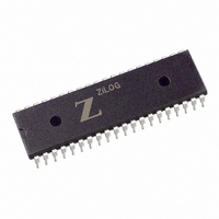
Z0847006PSG Zilog, Z0847006PSG Datasheet - Page 301

Z0847006PSG
Manufacturer Part Number
Z0847006PSG
Description
IC 6MHZ Z80 NMOS DART 40-DIP
Manufacturer
Zilog
Series
Z80r
Datasheet
1.Z0847006PSG.pdf
(330 pages)
Specifications of Z0847006PSG
Processor Type
Z80
Features
Dual Channel Asynchronous Receiver/Transmitter (DART)
Speed
6MHz
Voltage
5V
Mounting Type
Through Hole
Package / Case
40-DIP (0.620", 15.75mm)
Mounting Style
Through Hole
Cpu Speed
6MHz
Digital Ic Case Style
DIP
No. Of Pins
40
Supply Voltage Range
5V
Operating Temperature Range
0°C To +70°C
Svhc
No SVHC (18-Jun-2010)
Base Number
847006
Rohs Compliant
Yes
Clock Frequency
6MHz
Lead Free Status / RoHS Status
Lead free / RoHS Compliant
Available stocks
Company
Part Number
Manufacturer
Quantity
Price
Company:
Part Number:
Z0847006PSG
Manufacturer:
Zilog
Quantity:
22
- Current page: 301 of 330
- Download datasheet (3Mb)
UM008101-0601
IORQ and the corresponding S/A and C/D inputs to the Z80 SIO to
transfer data. The READY output becomes inactive when IORQ and CS
become active. The Ready function can occur internally in the Z80 SIO,
whether it is addressed or not. Therefore, the READY output becomes
inactive when any CPU data or command transfer occurs. Because the
DMA controller is not enabled when the CPU transfer occurs, the system
continues to function normally.
The Wait function is active only when the CPU attempts to read Z80 SIO
data that has not yet been received, which occurs frequently when block
transfer instructions are used. The Wait function can also become active
(under program control) if the CPU tries to write data while the transmit
buffer is still full. The WAIT output for either channel becomes active
when the opposite channel is addressed. This active state occurs because
the Z80 SIO is addressed and does not affect software loops or block move
instructions.
Write Register 2
WR2
only. V7-V4 and V0 are always returned exactly as written; V3-V1 are
returned as written if the Status Affects Vector (WR1, D2) control bit is 0. If
this bit is 1, they are modified as explained in
page
Table 19. Write Register 2 Interrupt Vector
D7
V7
277.
(Figure
D6
V6
116) is the interrupt vector register and occurs in Channel B
D5
V5
D4
V4
D3
V3
“Write Register 1” on
D2
V2
Z80 CPU Peripherals
Serial Input/Output
D1
V1
User Manual
D0
V0
281
Related parts for Z0847006PSG
Image
Part Number
Description
Manufacturer
Datasheet
Request
R

Part Number:
Description:
Customer Procurement Spec(CPS)
Manufacturer:
ZILOG [Zilog, Inc.]
Datasheet:

Part Number:
Description:
Communication Controllers, ZILOG INTELLIGENT PERIPHERAL CONTROLLER (ZIP)
Manufacturer:
Zilog, Inc.
Datasheet:

Part Number:
Description:
KIT DEV FOR Z8 ENCORE 16K TO 64K
Manufacturer:
Zilog
Datasheet:

Part Number:
Description:
KIT DEV Z8 ENCORE XP 28-PIN
Manufacturer:
Zilog
Datasheet:

Part Number:
Description:
DEV KIT FOR Z8 ENCORE 8K/4K
Manufacturer:
Zilog
Datasheet:

Part Number:
Description:
KIT DEV Z8 ENCORE XP 28-PIN
Manufacturer:
Zilog
Datasheet:

Part Number:
Description:
DEV KIT FOR Z8 ENCORE 4K TO 8K
Manufacturer:
Zilog
Datasheet:

Part Number:
Description:
CMOS Z8 microcontroller. ROM 16 Kbytes, RAM 256 bytes, speed 16 MHz, 32 lines I/O, 3.0V to 5.5V
Manufacturer:
Zilog, Inc.
Datasheet:

Part Number:
Description:
Low-cost microcontroller. 512 bytes ROM, 61 bytes RAM, 8 MHz
Manufacturer:
Zilog, Inc.
Datasheet:

Part Number:
Description:
Z8 4K OTP Microcontroller
Manufacturer:
Zilog, Inc.
Datasheet:

Part Number:
Description:
CMOS SUPER8 ROMLESS MCU
Manufacturer:
Zilog, Inc.
Datasheet:

Part Number:
Description:
SL1866 CMOSZ8 OTP Microcontroller
Manufacturer:
Zilog, Inc.
Datasheet:

Part Number:
Description:
SL1866 CMOSZ8 OTP Microcontroller
Manufacturer:
Zilog, Inc.
Datasheet:

Part Number:
Description:
OTP (KB) = 1, RAM = 125, Speed = 12, I/O = 14, 8-bit Timers = 2, Comm Interfaces Other Features = Por, LV Protect, Voltage = 4.5-5.5V
Manufacturer:
Zilog, Inc.
Datasheet:


