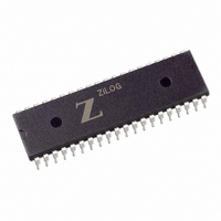
Z0847006PSG Zilog, Z0847006PSG Datasheet - Page 114

Z0847006PSG
Manufacturer Part Number
Z0847006PSG
Description
IC 6MHZ Z80 NMOS DART 40-DIP
Manufacturer
Zilog
Series
Z80r
Datasheet
1.Z0847006PSG.pdf
(330 pages)
Specifications of Z0847006PSG
Processor Type
Z80
Features
Dual Channel Asynchronous Receiver/Transmitter (DART)
Speed
6MHz
Voltage
5V
Mounting Type
Through Hole
Package / Case
40-DIP (0.620", 15.75mm)
Mounting Style
Through Hole
Cpu Speed
6MHz
Digital Ic Case Style
DIP
No. Of Pins
40
Supply Voltage Range
5V
Operating Temperature Range
0°C To +70°C
Svhc
No SVHC (18-Jun-2010)
Base Number
847006
Rohs Compliant
Yes
Clock Frequency
6MHz
Lead Free Status / RoHS Status
Lead free / RoHS Compliant
Available stocks
Company
Part Number
Manufacturer
Quantity
Price
Company:
Part Number:
Z0847006PSG
Manufacturer:
Zilog
Quantity:
22
- Current page: 114 of 330
- Download datasheet (3Mb)
UM008101-0601
< % 2 7 2 G T K R J G T C N U
7 U G T / C P W C N
Write Register 1 Group
Bits 7, 2, 1, and 0, as Figure 41 illustrates, select the base register byte for
this group. The group is used only when Port A is used, for example, do not
program it for a search only, simultaneous transfer, or simultaneous transfer/
search with Port B as the source. It specifies the following characteristics:
Device Type (Port A)
Bit 3 identifies Port A as either memory or I/O. This specification causes
the proper control line MREQ or IORQ to come active for cycles involving
that port.
Variable/Fixed Addressing (Port A)
Bits 4 and 5 specify whether the Port A address increments, decrements, or
remains fixed for each byte of data transferred or searched. The first byte of
data in an operation uses the starting address entered for Port A in WR0.
Incrementing or decrementing begins on the second byte of the operation.
Variable Cycle (Port A)
If bit 6 is set to 0, the DMA’s variable-cycle timing feature is not used;
instead, standard Z80 timing for read and write cycles is used, which is
described in the “Timing” chapter. If bit 6 is set to 1, the next byte written
to the DMA after the WR1 base register byte is the Port A variable-timing
byte. This allows the length of the port’s read and write cycles to be
shortened. The choices for overall cycle timing of the DMA, including
activation of the IORQ, MREQ, RD, and WR lines, are specified in bits 1
and 0 as follows:
4 clock cycles
3 clock cycles
2 clock cycles
Direct Memory Access
Related parts for Z0847006PSG
Image
Part Number
Description
Manufacturer
Datasheet
Request
R

Part Number:
Description:
Customer Procurement Spec(CPS)
Manufacturer:
ZILOG [Zilog, Inc.]
Datasheet:

Part Number:
Description:
Communication Controllers, ZILOG INTELLIGENT PERIPHERAL CONTROLLER (ZIP)
Manufacturer:
Zilog, Inc.
Datasheet:

Part Number:
Description:
KIT DEV FOR Z8 ENCORE 16K TO 64K
Manufacturer:
Zilog
Datasheet:

Part Number:
Description:
KIT DEV Z8 ENCORE XP 28-PIN
Manufacturer:
Zilog
Datasheet:

Part Number:
Description:
DEV KIT FOR Z8 ENCORE 8K/4K
Manufacturer:
Zilog
Datasheet:

Part Number:
Description:
KIT DEV Z8 ENCORE XP 28-PIN
Manufacturer:
Zilog
Datasheet:

Part Number:
Description:
DEV KIT FOR Z8 ENCORE 4K TO 8K
Manufacturer:
Zilog
Datasheet:

Part Number:
Description:
CMOS Z8 microcontroller. ROM 16 Kbytes, RAM 256 bytes, speed 16 MHz, 32 lines I/O, 3.0V to 5.5V
Manufacturer:
Zilog, Inc.
Datasheet:

Part Number:
Description:
Low-cost microcontroller. 512 bytes ROM, 61 bytes RAM, 8 MHz
Manufacturer:
Zilog, Inc.
Datasheet:

Part Number:
Description:
Z8 4K OTP Microcontroller
Manufacturer:
Zilog, Inc.
Datasheet:

Part Number:
Description:
CMOS SUPER8 ROMLESS MCU
Manufacturer:
Zilog, Inc.
Datasheet:

Part Number:
Description:
SL1866 CMOSZ8 OTP Microcontroller
Manufacturer:
Zilog, Inc.
Datasheet:

Part Number:
Description:
SL1866 CMOSZ8 OTP Microcontroller
Manufacturer:
Zilog, Inc.
Datasheet:

Part Number:
Description:
OTP (KB) = 1, RAM = 125, Speed = 12, I/O = 14, 8-bit Timers = 2, Comm Interfaces Other Features = Por, LV Protect, Voltage = 4.5-5.5V
Manufacturer:
Zilog, Inc.
Datasheet:


