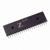
Z0847006PSG Zilog, Z0847006PSG Datasheet - Page 151

Z0847006PSG
Manufacturer Part Number
Z0847006PSG
Description
IC 6MHZ Z80 NMOS DART 40-DIP
Manufacturer
Zilog
Series
Z80r
Datasheet
1.Z0847006PSG.pdf
(330 pages)
Specifications of Z0847006PSG
Processor Type
Z80
Features
Dual Channel Asynchronous Receiver/Transmitter (DART)
Speed
6MHz
Voltage
5V
Mounting Type
Through Hole
Package / Case
40-DIP (0.620", 15.75mm)
Mounting Style
Through Hole
Cpu Speed
6MHz
Digital Ic Case Style
DIP
No. Of Pins
40
Supply Voltage Range
5V
Operating Temperature Range
0°C To +70°C
Svhc
No SVHC (18-Jun-2010)
Base Number
847006
Rohs Compliant
Yes
Clock Frequency
6MHz
Lead Free Status / RoHS Status
Lead free / RoHS Compliant
Available stocks
Company
Part Number
Manufacturer
Quantity
Price
Company:
Part Number:
Z0847006PSG
Manufacturer:
Zilog
Quantity:
22
- Current page: 151 of 330
- Download datasheet (3Mb)
< % 2 7 2 G T K R J G T C N U
7 U G T / C P W C N
CPU has relinquished the bus. Therefore, if this DMA is bus master, it
samples the WAIT signal for these requests. A simple 2-input multiplexer
steers the CE/WAIT signals as depicted in Figure 50. Using BUSACK
assumes that there is only one DMA. In systems with three or more
possible bus masters, BAl active and BAO inactive identify the master.
Simultaneous Transfers
The highest-speed DMA transfer method is the simultaneous transfer
method, or flyby method. This requires some external hardware to
generate simultaneous read- and write-control signals to the source and
destination ports.
Because the address bus is used for memory address, only transfers
between I/O and memory can be accomplished directly when the I/O port
selection is performed by hard wiring. The DMA is put into search mode,
and a circuit, such as that illustrated in Figure 51, generates separate simul-
taneous read- and write-control signals, which may be ORed into the read-
and write-control paths at memory and I/O. Figure 52 depicts such an
arrangement. This arrangement allows both the CPU and DMA access to
the I/O peripheral. (If the peripheral communicates only through DMA, it
only needs to use the IORD and IOWR signals.)
Pay careful attention to access, setup, and hold times in this mode. Because
the DMA is programmed to do searching, the MWR and IOWR signals are
derived from the DMA RD signal and mimic its timing. This does not cause
a problem for write operations, which are trailing edge activated. To make
MWR appear more like a CPU or DMA write cycle signal, the circuit of
Figure 50 may be used to delay the leading edge of MWR until after the
falling edge in T2. The programmable variable timing features of the DMA
may be useful, too.
UM008101-0601
Direct Memory Access
Related parts for Z0847006PSG
Image
Part Number
Description
Manufacturer
Datasheet
Request
R

Part Number:
Description:
Customer Procurement Spec(CPS)
Manufacturer:
ZILOG [Zilog, Inc.]
Datasheet:

Part Number:
Description:
Communication Controllers, ZILOG INTELLIGENT PERIPHERAL CONTROLLER (ZIP)
Manufacturer:
Zilog, Inc.
Datasheet:

Part Number:
Description:
KIT DEV FOR Z8 ENCORE 16K TO 64K
Manufacturer:
Zilog
Datasheet:

Part Number:
Description:
KIT DEV Z8 ENCORE XP 28-PIN
Manufacturer:
Zilog
Datasheet:

Part Number:
Description:
DEV KIT FOR Z8 ENCORE 8K/4K
Manufacturer:
Zilog
Datasheet:

Part Number:
Description:
KIT DEV Z8 ENCORE XP 28-PIN
Manufacturer:
Zilog
Datasheet:

Part Number:
Description:
DEV KIT FOR Z8 ENCORE 4K TO 8K
Manufacturer:
Zilog
Datasheet:

Part Number:
Description:
CMOS Z8 microcontroller. ROM 16 Kbytes, RAM 256 bytes, speed 16 MHz, 32 lines I/O, 3.0V to 5.5V
Manufacturer:
Zilog, Inc.
Datasheet:

Part Number:
Description:
Low-cost microcontroller. 512 bytes ROM, 61 bytes RAM, 8 MHz
Manufacturer:
Zilog, Inc.
Datasheet:

Part Number:
Description:
Z8 4K OTP Microcontroller
Manufacturer:
Zilog, Inc.
Datasheet:

Part Number:
Description:
CMOS SUPER8 ROMLESS MCU
Manufacturer:
Zilog, Inc.
Datasheet:

Part Number:
Description:
SL1866 CMOSZ8 OTP Microcontroller
Manufacturer:
Zilog, Inc.
Datasheet:

Part Number:
Description:
SL1866 CMOSZ8 OTP Microcontroller
Manufacturer:
Zilog, Inc.
Datasheet:

Part Number:
Description:
OTP (KB) = 1, RAM = 125, Speed = 12, I/O = 14, 8-bit Timers = 2, Comm Interfaces Other Features = Por, LV Protect, Voltage = 4.5-5.5V
Manufacturer:
Zilog, Inc.
Datasheet:


