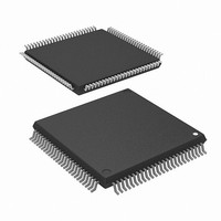
R5F2L3AAANFP#U1 Renesas Electronics America, R5F2L3AAANFP#U1 Datasheet - Page 159

R5F2L3AAANFP#U1
Manufacturer Part Number
R5F2L3AAANFP#U1
Description
MCU FLASH 96+4KB 100LQFP
Manufacturer
Renesas Electronics America
Series
R8C/Lx/3AAr
Datasheet
1.R5F2L387ANFPU1.pdf
(864 pages)
Specifications of R5F2L3AAANFP#U1
Core Processor
R8C
Core Size
16/32-Bit
Speed
20MHz
Connectivity
I²C, LIN, SIO, SSU, UART/USART
Peripherals
LCD, POR, PWM, Voltage Detect, WDT
Number Of I /o
88
Program Memory Size
96KB (96K x 8)
Program Memory Type
FLASH
Ram Size
10K x 8
Voltage - Supply (vcc/vdd)
1.8 V ~ 5.5 V
Data Converters
A/D 20x10b; D/A 2x8b
Oscillator Type
Internal
Operating Temperature
-20°C ~ 85°C
Package / Case
100-LQFP
Lead Free Status / RoHS Status
Lead free / RoHS Compliant
Eeprom Size
-
Available stocks
Company
Part Number
Manufacturer
Quantity
Price
- Current page: 159 of 864
- Download datasheet (16Mb)
R8C/L35A Group, R8C/L36A Group, R8C/L38A Group, R8C/L3AA Group,
R8C/L35B Group, R8C/L36B Group, R8C/L38B Group, R8C/L3AB Group
REJ09B0441-0100 Rev.1.00
Page 122 of 802
8.8
8.8.1
8.8.2
8.8.3
8.8.4
To use the XCIN clock, set the CM03 bit to 1 once and then set it to 0 (XCIN clock oscillates). To use the VL1
internally-generated voltage in the LCD drive control circuit, set the LVURS bit in the LCR1 register to 1 (VL1
internally-generated voltage) after the above setting.
Since the oscillation stop detection function cannot be used when the XIN clock frequency is below 2 MHz, set
bits OCD1 to OCD0 to 00b.
Consult the oscillator manufacturer to determine the optimal oscillation circuit constants for the user system.
The P12_0 pin is shared with the XIN pin, and the P12_1 pin is shared with the XOUT pin. These pins cannot
be used as I/O ports when using the XIN clock.
Notes on Clock Generation Circuit
Oscillation Stop Detection Function
Oscillation Circuit Constants
XCIN Clock
Notes on Using Pins P12_0 and P12_1
Oct 30, 2009
8. Clock Generation Circuit
Related parts for R5F2L3AAANFP#U1
Image
Part Number
Description
Manufacturer
Datasheet
Request
R

Part Number:
Description:
KIT STARTER FOR M16C/29
Manufacturer:
Renesas Electronics America
Datasheet:

Part Number:
Description:
KIT STARTER FOR R8C/2D
Manufacturer:
Renesas Electronics America
Datasheet:

Part Number:
Description:
R0K33062P STARTER KIT
Manufacturer:
Renesas Electronics America
Datasheet:

Part Number:
Description:
KIT STARTER FOR R8C/23 E8A
Manufacturer:
Renesas Electronics America
Datasheet:

Part Number:
Description:
KIT STARTER FOR R8C/25
Manufacturer:
Renesas Electronics America
Datasheet:

Part Number:
Description:
KIT STARTER H8S2456 SHARPE DSPLY
Manufacturer:
Renesas Electronics America
Datasheet:

Part Number:
Description:
KIT STARTER FOR R8C38C
Manufacturer:
Renesas Electronics America
Datasheet:

Part Number:
Description:
KIT STARTER FOR R8C35C
Manufacturer:
Renesas Electronics America
Datasheet:

Part Number:
Description:
KIT STARTER FOR R8CL3AC+LCD APPS
Manufacturer:
Renesas Electronics America
Datasheet:

Part Number:
Description:
KIT STARTER FOR RX610
Manufacturer:
Renesas Electronics America
Datasheet:

Part Number:
Description:
KIT STARTER FOR R32C/118
Manufacturer:
Renesas Electronics America
Datasheet:

Part Number:
Description:
KIT DEV RSK-R8C/26-29
Manufacturer:
Renesas Electronics America
Datasheet:

Part Number:
Description:
KIT STARTER FOR SH7124
Manufacturer:
Renesas Electronics America
Datasheet:

Part Number:
Description:
KIT STARTER FOR H8SX/1622
Manufacturer:
Renesas Electronics America
Datasheet:

Part Number:
Description:
KIT DEV FOR SH7203
Manufacturer:
Renesas Electronics America
Datasheet:


