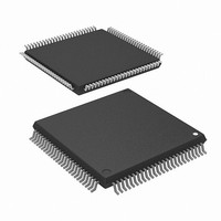
R5F2L3AAANFP#U1 Renesas Electronics America, R5F2L3AAANFP#U1 Datasheet - Page 495

R5F2L3AAANFP#U1
Manufacturer Part Number
R5F2L3AAANFP#U1
Description
MCU FLASH 96+4KB 100LQFP
Manufacturer
Renesas Electronics America
Series
R8C/Lx/3AAr
Datasheet
1.R5F2L387ANFPU1.pdf
(864 pages)
Specifications of R5F2L3AAANFP#U1
Core Processor
R8C
Core Size
16/32-Bit
Speed
20MHz
Connectivity
I²C, LIN, SIO, SSU, UART/USART
Peripherals
LCD, POR, PWM, Voltage Detect, WDT
Number Of I /o
88
Program Memory Size
96KB (96K x 8)
Program Memory Type
FLASH
Ram Size
10K x 8
Voltage - Supply (vcc/vdd)
1.8 V ~ 5.5 V
Data Converters
A/D 20x10b; D/A 2x8b
Oscillator Type
Internal
Operating Temperature
-20°C ~ 85°C
Package / Case
100-LQFP
Lead Free Status / RoHS Status
Lead free / RoHS Compliant
Eeprom Size
-
Available stocks
Company
Part Number
Manufacturer
Quantity
Price
- Current page: 495 of 864
- Download datasheet (16Mb)
R8C/L35A Group, R8C/L36A Group, R8C/L38A Group, R8C/L3AA Group,
R8C/L35B Group, R8C/L36B Group, R8C/L38B Group, R8C/L3AB Group
REJ09B0441-0100 Rev.1.00
Page 458 of 802
Figure 22.5
22.3.3
TRGIOj input signal
TRGCLKA
TRGCLKB
TRGIOj input signal
Input signal after
passing through
Sampling clock
f32
The input to TRGIOj (j = A or B) is sampled and the level is determined when three matches occur. The digital
filter function and sampling clock are selected by using the TRGMR register.
Figure 22.5 shows a Block Diagram of Digital Filter.
f1
f4
f8
digital filter
Digital Filter
TCK0 to TCK2: Bits in TRGCR register
DFCK0, DFCK1, DFj: Bits in TRGMR register
IOA0 to IOA2, IOB0 to IOB2: Bits in TRGIOR register
j = A or B
Clock cycle selected by
= 011b
= 100b
Timer RG operating clock
(or DFCK1 to DFCK0)
= 010b
= 101b
TCK2 to TCK0
Block Diagram of Digital Filter
D
D
Latch
Latch
C
TCK2 to TCK0
f1
C
= 111b
Q
Q
= 000b
Count source
D
Oct 30, 2009
f32
f8
f1
Latch
C
If fewer than three matches occur,
the matches are recognized as noise
and no transmission is performed.
= 01b
= 10b
= 00b
= 11b
DFCK1 to DFCK0
Q
D
Latch
C
Sampling clock
Q
D
Latch
C
Q
detection
Maximum signal transmission
delay is five sampling clocks.
a signal change is confirmed.
Match
circuit
Three matches occur and
DFj
1
0
IOA2 to IOA0
IOB2 to IOB0
detection
circuit
Edge
22. Timer RG
Related parts for R5F2L3AAANFP#U1
Image
Part Number
Description
Manufacturer
Datasheet
Request
R

Part Number:
Description:
KIT STARTER FOR M16C/29
Manufacturer:
Renesas Electronics America
Datasheet:

Part Number:
Description:
KIT STARTER FOR R8C/2D
Manufacturer:
Renesas Electronics America
Datasheet:

Part Number:
Description:
R0K33062P STARTER KIT
Manufacturer:
Renesas Electronics America
Datasheet:

Part Number:
Description:
KIT STARTER FOR R8C/23 E8A
Manufacturer:
Renesas Electronics America
Datasheet:

Part Number:
Description:
KIT STARTER FOR R8C/25
Manufacturer:
Renesas Electronics America
Datasheet:

Part Number:
Description:
KIT STARTER H8S2456 SHARPE DSPLY
Manufacturer:
Renesas Electronics America
Datasheet:

Part Number:
Description:
KIT STARTER FOR R8C38C
Manufacturer:
Renesas Electronics America
Datasheet:

Part Number:
Description:
KIT STARTER FOR R8C35C
Manufacturer:
Renesas Electronics America
Datasheet:

Part Number:
Description:
KIT STARTER FOR R8CL3AC+LCD APPS
Manufacturer:
Renesas Electronics America
Datasheet:

Part Number:
Description:
KIT STARTER FOR RX610
Manufacturer:
Renesas Electronics America
Datasheet:

Part Number:
Description:
KIT STARTER FOR R32C/118
Manufacturer:
Renesas Electronics America
Datasheet:

Part Number:
Description:
KIT DEV RSK-R8C/26-29
Manufacturer:
Renesas Electronics America
Datasheet:

Part Number:
Description:
KIT STARTER FOR SH7124
Manufacturer:
Renesas Electronics America
Datasheet:

Part Number:
Description:
KIT STARTER FOR H8SX/1622
Manufacturer:
Renesas Electronics America
Datasheet:

Part Number:
Description:
KIT DEV FOR SH7203
Manufacturer:
Renesas Electronics America
Datasheet:


