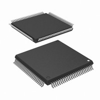
R5F2L3AAANFP#U1 Renesas Electronics America, R5F2L3AAANFP#U1 Datasheet - Page 860

R5F2L3AAANFP#U1
Manufacturer Part Number
R5F2L3AAANFP#U1
Description
MCU FLASH 96+4KB 100LQFP
Manufacturer
Renesas Electronics America
Series
R8C/Lx/3AAr
Datasheet
1.R5F2L387ANFPU1.pdf
(864 pages)
Specifications of R5F2L3AAANFP#U1
Core Processor
R8C
Core Size
16/32-Bit
Speed
20MHz
Connectivity
I²C, LIN, SIO, SSU, UART/USART
Peripherals
LCD, POR, PWM, Voltage Detect, WDT
Number Of I /o
88
Program Memory Size
96KB (96K x 8)
Program Memory Type
FLASH
Ram Size
10K x 8
Voltage - Supply (vcc/vdd)
1.8 V ~ 5.5 V
Data Converters
A/D 20x10b; D/A 2x8b
Oscillator Type
Internal
Operating Temperature
-20°C ~ 85°C
Package / Case
100-LQFP
Lead Free Status / RoHS Status
Lead free / RoHS Compliant
Eeprom Size
-
Available stocks
Company
Part Number
Manufacturer
Quantity
Price
- Current page: 860 of 864
- Download datasheet (16Mb)
Nippon Bldg., 2-6-2, Ohte-machi, Chiyoda-ku, Tokyo 100-0004, Japan
Renesas Technology Corp.
Applicable
The following notes are pertinent to the manuals listed above. Refer to individual hardware manuals to ascertain which Series
have the functions shown below.
1.
2.
3.
(c) 2009. Renesas Technology Corp., All rights reserved.
Category
Products
Product
Title
Note on voltage monitor interrupt and voltage monitor reset
(This note applies to MCUs that have the voltage change detection flag.)
When the voltage detection circuit is enabled while the voltage monitor interrupt or voltage monitor reset is disabled, low
voltage is detected and the voltage change detection flag becomes 1. When low voltage is detected after the voltage
detection circuit is enabled until an interrupt or a reset is enabled for the setting procedure of bits associated with voltage
monitor interrupt or bits associated with voltage monitor reset, an interrupt or a reset is not generated. After an interrupt or
a rest is enabled, read the voltage change detection flag. When the flag is read as 1, perform the process that occurs
when low voltage is detected.
Note when entering wait mode by wait control bit (CM30 bit)
(The R8C/1x Series and R8C/2x Series do not have the CM30 bit.)
As with executing the WAIT instruction, insert at least four NOP instructions after the instruction that sets the CM30 bit to 1.
Program example to set the CM30 bit to 1
Note on INTi pin
(All INT pins apply to this note. The value for i varies according to the MCU.)
As with changing the INT interrupt polarity select bit (INTiPL bit), when changing the INT input enable bit (INTiEN bit), the
IR bit corresponding to the INTi pin may become 1 (interrupt requested). Refer to Changing Interrupt Sources in the
hardware manual.
BCLR 1, FMR0
BSET 0, PRCR
FCLR I
BSET 0, CM3
NOP
NOP
NOP
NOP
BCLR 0, PRCR
FSET I
MPU/MCU
Notes on R8C Family
R8C/1x Series
R8C/2x Series
R8C/3x Series
R8C/Lx Series
RENESAS TECHNICAL UPDATE
Lot No.
Information
Reference
Document
Document
Category
No.
TN-R8C-A007A/E
Technical Notification
Date: Sep.25, 2009
Rev.
Page 1 of 3
1.00
Related parts for R5F2L3AAANFP#U1
Image
Part Number
Description
Manufacturer
Datasheet
Request
R

Part Number:
Description:
KIT STARTER FOR M16C/29
Manufacturer:
Renesas Electronics America
Datasheet:

Part Number:
Description:
KIT STARTER FOR R8C/2D
Manufacturer:
Renesas Electronics America
Datasheet:

Part Number:
Description:
R0K33062P STARTER KIT
Manufacturer:
Renesas Electronics America
Datasheet:

Part Number:
Description:
KIT STARTER FOR R8C/23 E8A
Manufacturer:
Renesas Electronics America
Datasheet:

Part Number:
Description:
KIT STARTER FOR R8C/25
Manufacturer:
Renesas Electronics America
Datasheet:

Part Number:
Description:
KIT STARTER H8S2456 SHARPE DSPLY
Manufacturer:
Renesas Electronics America
Datasheet:

Part Number:
Description:
KIT STARTER FOR R8C38C
Manufacturer:
Renesas Electronics America
Datasheet:

Part Number:
Description:
KIT STARTER FOR R8C35C
Manufacturer:
Renesas Electronics America
Datasheet:

Part Number:
Description:
KIT STARTER FOR R8CL3AC+LCD APPS
Manufacturer:
Renesas Electronics America
Datasheet:

Part Number:
Description:
KIT STARTER FOR RX610
Manufacturer:
Renesas Electronics America
Datasheet:

Part Number:
Description:
KIT STARTER FOR R32C/118
Manufacturer:
Renesas Electronics America
Datasheet:

Part Number:
Description:
KIT DEV RSK-R8C/26-29
Manufacturer:
Renesas Electronics America
Datasheet:

Part Number:
Description:
KIT STARTER FOR SH7124
Manufacturer:
Renesas Electronics America
Datasheet:

Part Number:
Description:
KIT STARTER FOR H8SX/1622
Manufacturer:
Renesas Electronics America
Datasheet:

Part Number:
Description:
KIT DEV FOR SH7203
Manufacturer:
Renesas Electronics America
Datasheet:


