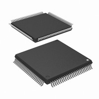
R5F2L3AAANFP#U1 Renesas Electronics America, R5F2L3AAANFP#U1 Datasheet - Page 179

R5F2L3AAANFP#U1
Manufacturer Part Number
R5F2L3AAANFP#U1
Description
MCU FLASH 96+4KB 100LQFP
Manufacturer
Renesas Electronics America
Series
R8C/Lx/3AAr
Datasheet
1.R5F2L387ANFPU1.pdf
(864 pages)
Specifications of R5F2L3AAANFP#U1
Core Processor
R8C
Core Size
16/32-Bit
Speed
20MHz
Connectivity
I²C, LIN, SIO, SSU, UART/USART
Peripherals
LCD, POR, PWM, Voltage Detect, WDT
Number Of I /o
88
Program Memory Size
96KB (96K x 8)
Program Memory Type
FLASH
Ram Size
10K x 8
Voltage - Supply (vcc/vdd)
1.8 V ~ 5.5 V
Data Converters
A/D 20x10b; D/A 2x8b
Oscillator Type
Internal
Operating Temperature
-20°C ~ 85°C
Package / Case
100-LQFP
Lead Free Status / RoHS Status
Lead free / RoHS Compliant
Eeprom Size
-
Available stocks
Company
Part Number
Manufacturer
Quantity
Price
- Current page: 179 of 864
- Download datasheet (16Mb)
R8C/L35A Group, R8C/L36A Group, R8C/L38A Group, R8C/L3AA Group,
R8C/L35B Group, R8C/L36B Group, R8C/L38B Group, R8C/L3AB Group
REJ09B0441-0100 Rev.1.00
Page 142 of 802
Figure 9.7
9.7.6
9.7.7
9.7.8
Step (1)
Step (2)
Step (3)
Step (4)
Step (5)
Step (6)
Step (7)
Step (8)
Notes:
VCA20: Bit in VCA2 register
1. Execute this routine to handle all interrupts generated in wait mode.
2. Do not set the VCA20 bit to 0 with the instruction immediately after setting the VCA20 bit to 1. Also, do not do the opposite.
3. When the VCA20 bit is set to 1, do not set the CM10 bit to 1 (stop mode).
4. When the MCU enters wait mode, follow 9.4 Wait Mode.
When the A/D converter is not used, power consumption can be reduced by setting the ADSTBY bit in the
ADCON1 register to 0 (A/D operation stops (standby)) to shut off any analog circuit current flow.
When the SSU or I
When the MCU enters wait mode using low-speed clock mode or low-speed on-chip oscillator mode, internal
power consumption can be reduced by using the VCA20 bit in the VCA2 register. Figure 9.7 shows the
Handling Procedure for Reducing Internal Power Consumption Using VCA20 Bit. To enable reduced internal
power consumption by the VCA20 bit, follow this procedure.
However, this does not apply if it is not necessary to start the high-speed clock during the interrupt routine.
(internal power low consumption enabled)
(Wait until the XIN clock oscillation stabilizes)
(internal power low consumption disabled)
power consumption using the VCA20 bit
Procedure for enabling reduced internal
A/D Converter
Clock Synchronous Serial Interface
Reducing Internal Power Consumption
low-speed on-chip oscillator mode
Enter low-speed clock mode or
Enter high-speed clock mode
Handling Procedure for Reducing Internal Power Consumption Using VCA20 Bit
Enter wait mode
Start the XIN clock
Stop the XIN clock
VCA20
VCA20
2
C bus is not used, set the MSTIIC bit in the MSTCR register to 1 (standby).
1
0
(4)
Oct 30, 2009
(2, 3)
(2)
Exit wait mode by interrupt
Step (5)
Step (6)
Step (7)
Step (8)
Step (1)
Step (2)
Step (3)
(internal power low consumption enabled)
(Wait until the XIN clock oscillation stabilizes)
(internal power low consumption disabled)
low-speed on-chip oscillator mode
Enter low-speed clock mode or
Enter high-speed clock mode
Interrupt handling completed
In the interrupt routine
Start the XIN clock
Stop the XIN clock
Interrupt handling
VCA20
VCA20
0
1
(Note 1)
(2, 3)
(2)
If it is necessary to start
the high-speed clock during
the interrupt routine, execute
steps (6) and (7) in the
routine.
If the high-speed clock starts
during the interrupt routine,
execute steps (1) to (3) at
the end of the routine.
9. Power Control
Related parts for R5F2L3AAANFP#U1
Image
Part Number
Description
Manufacturer
Datasheet
Request
R

Part Number:
Description:
KIT STARTER FOR M16C/29
Manufacturer:
Renesas Electronics America
Datasheet:

Part Number:
Description:
KIT STARTER FOR R8C/2D
Manufacturer:
Renesas Electronics America
Datasheet:

Part Number:
Description:
R0K33062P STARTER KIT
Manufacturer:
Renesas Electronics America
Datasheet:

Part Number:
Description:
KIT STARTER FOR R8C/23 E8A
Manufacturer:
Renesas Electronics America
Datasheet:

Part Number:
Description:
KIT STARTER FOR R8C/25
Manufacturer:
Renesas Electronics America
Datasheet:

Part Number:
Description:
KIT STARTER H8S2456 SHARPE DSPLY
Manufacturer:
Renesas Electronics America
Datasheet:

Part Number:
Description:
KIT STARTER FOR R8C38C
Manufacturer:
Renesas Electronics America
Datasheet:

Part Number:
Description:
KIT STARTER FOR R8C35C
Manufacturer:
Renesas Electronics America
Datasheet:

Part Number:
Description:
KIT STARTER FOR R8CL3AC+LCD APPS
Manufacturer:
Renesas Electronics America
Datasheet:

Part Number:
Description:
KIT STARTER FOR RX610
Manufacturer:
Renesas Electronics America
Datasheet:

Part Number:
Description:
KIT STARTER FOR R32C/118
Manufacturer:
Renesas Electronics America
Datasheet:

Part Number:
Description:
KIT DEV RSK-R8C/26-29
Manufacturer:
Renesas Electronics America
Datasheet:

Part Number:
Description:
KIT STARTER FOR SH7124
Manufacturer:
Renesas Electronics America
Datasheet:

Part Number:
Description:
KIT STARTER FOR H8SX/1622
Manufacturer:
Renesas Electronics America
Datasheet:

Part Number:
Description:
KIT DEV FOR SH7203
Manufacturer:
Renesas Electronics America
Datasheet:


