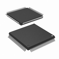
R5F2L3AAANFP#U1 Renesas Electronics America, R5F2L3AAANFP#U1 Datasheet - Page 850

R5F2L3AAANFP#U1
Manufacturer Part Number
R5F2L3AAANFP#U1
Description
MCU FLASH 96+4KB 100LQFP
Manufacturer
Renesas Electronics America
Series
R8C/Lx/3AAr
Datasheet
1.R5F2L387ANFPU1.pdf
(864 pages)
Specifications of R5F2L3AAANFP#U1
Core Processor
R8C
Core Size
16/32-Bit
Speed
20MHz
Connectivity
I²C, LIN, SIO, SSU, UART/USART
Peripherals
LCD, POR, PWM, Voltage Detect, WDT
Number Of I /o
88
Program Memory Size
96KB (96K x 8)
Program Memory Type
FLASH
Ram Size
10K x 8
Voltage - Supply (vcc/vdd)
1.8 V ~ 5.5 V
Data Converters
A/D 20x10b; D/A 2x8b
Oscillator Type
Internal
Operating Temperature
-20°C ~ 85°C
Package / Case
100-LQFP
Lead Free Status / RoHS Status
Lead free / RoHS Compliant
Eeprom Size
-
Available stocks
Company
Part Number
Manufacturer
Quantity
Price
- Current page: 850 of 864
- Download datasheet (16Mb)
1.00
Rev.
REVISION HISTORY
Oct 30, 2009
Date
142 to 144 Figure 9.7 to Figure 9.9 revised
146, 752 9.8.3, 35.2.3 Power-Off Mode revised, 9.8.4, 35.2.4 Reducing Current added
184, 756 12.5.1, 35.4.1 revised
188, 756 13.3.1, 35.5.1 revised
Page
129
130
131
132
134
137
139
141
147
148
150
151
152
153
154
158
161
162
181
182
192
202
The last 9.2.5 FRA0 deleted, 9.2.5 After Reset, b1 to b7 revised, Note 3
to Note 5 deleted
9.2.6 Note 2 added
Table 9.2 “High-speed on-chip oscillator mode”, “FRA0 Register” deleted,
High-speed clock mode CM05, Low-speed clock mode CM04 revised
9.3.1 to 9.3.2 revised, the last 9.3.3 High-Speed On-Chip Oscillator
Mode deleted, 9.3.3 revised
Table 9.3 “Synchronous serial communication unit interrupt” “Synchronous serial
communication unit/I
interrupt” revised, “Voltage monitor 1”, “Voltage monitor 2”, “Watchdog timer interrupt”,
“Comparator A1 interrupt”, “Comparator A2 interrupt”, “LCD counter interrupt” deleted
Table 9.4 “INT0 to INT4”
“Voltage monitor 2 interrupt”, “Comparator A1 interrupt”, “Comparator A2
interrupt” deleted
Figure 9.5 revised
The last 9.7.1 Voltage Detection Circuit deleted,
9.7.1 “Unnecessary ports should be set to input and fixed... or stop mode.”
9.7.2 revised
10. Protection, 10.1.1 “FRA0, FRA1, FRA2, and FRA3”, “VD1LS, VW0C,
VW1C” deleted
Figure 11.1 revised
The last 11.1.3.3 Voltage Monitor 1/Comparator A1 Interrupt to 11.1.3.4
Voltage Monitor 2/Comparator A2 Interrupt deleted
Table 11.1 revised
Table 11.2 revised
11.2.1 “VCMP1IC”, “VCMP2IC” deleted
11.2.2 b3 (1) deleted
Table 11.5 revised
Figure 11.7 revised
Figure 11.8 revised
Figure 12.1 revised
12.2 “As the ID code areas are allocated in ... when creating a program.”
SFRs. Set appropriate values as ROM data by a program.”
14.2.4 “01b” (0FFFh): b8 to b3
“11b” (3FFFh): b10 to b5
Table 15.2 revised
R8C/L35A Group, R8C/L35B Group, R8C/L36A Group, R8C/L36B Group, R8C/L38A Group,
R8C/L38B Group, R8C/L3AA Group, R8C/L3AB Group Hardware Manual
“Unnecessary ports should be set to output. When...or stop mode.”,
“The ID code areas are allocated in the flash memory, not in the
C - 11
2
C bus interface interrupt”, “fOCO”
Description
b9 to b4
“INT0 to INT7”, “Voltage monitor 1 interrupt”,
b7 to b2, “10b” (1FFFh): b9 to b4
Summary
“fOCO-S”, “Timer RD
b8 to b3,
Related parts for R5F2L3AAANFP#U1
Image
Part Number
Description
Manufacturer
Datasheet
Request
R

Part Number:
Description:
KIT STARTER FOR M16C/29
Manufacturer:
Renesas Electronics America
Datasheet:

Part Number:
Description:
KIT STARTER FOR R8C/2D
Manufacturer:
Renesas Electronics America
Datasheet:

Part Number:
Description:
R0K33062P STARTER KIT
Manufacturer:
Renesas Electronics America
Datasheet:

Part Number:
Description:
KIT STARTER FOR R8C/23 E8A
Manufacturer:
Renesas Electronics America
Datasheet:

Part Number:
Description:
KIT STARTER FOR R8C/25
Manufacturer:
Renesas Electronics America
Datasheet:

Part Number:
Description:
KIT STARTER H8S2456 SHARPE DSPLY
Manufacturer:
Renesas Electronics America
Datasheet:

Part Number:
Description:
KIT STARTER FOR R8C38C
Manufacturer:
Renesas Electronics America
Datasheet:

Part Number:
Description:
KIT STARTER FOR R8C35C
Manufacturer:
Renesas Electronics America
Datasheet:

Part Number:
Description:
KIT STARTER FOR R8CL3AC+LCD APPS
Manufacturer:
Renesas Electronics America
Datasheet:

Part Number:
Description:
KIT STARTER FOR RX610
Manufacturer:
Renesas Electronics America
Datasheet:

Part Number:
Description:
KIT STARTER FOR R32C/118
Manufacturer:
Renesas Electronics America
Datasheet:

Part Number:
Description:
KIT DEV RSK-R8C/26-29
Manufacturer:
Renesas Electronics America
Datasheet:

Part Number:
Description:
KIT STARTER FOR SH7124
Manufacturer:
Renesas Electronics America
Datasheet:

Part Number:
Description:
KIT STARTER FOR H8SX/1622
Manufacturer:
Renesas Electronics America
Datasheet:

Part Number:
Description:
KIT DEV FOR SH7203
Manufacturer:
Renesas Electronics America
Datasheet:


