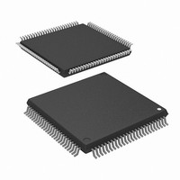
R5F2L3AAANFP#U1 Renesas Electronics America, R5F2L3AAANFP#U1 Datasheet - Page 39

R5F2L3AAANFP#U1
Manufacturer Part Number
R5F2L3AAANFP#U1
Description
MCU FLASH 96+4KB 100LQFP
Manufacturer
Renesas Electronics America
Series
R8C/Lx/3AAr
Datasheet
1.R5F2L387ANFPU1.pdf
(864 pages)
Specifications of R5F2L3AAANFP#U1
Core Processor
R8C
Core Size
16/32-Bit
Speed
20MHz
Connectivity
I²C, LIN, SIO, SSU, UART/USART
Peripherals
LCD, POR, PWM, Voltage Detect, WDT
Number Of I /o
88
Program Memory Size
96KB (96K x 8)
Program Memory Type
FLASH
Ram Size
10K x 8
Voltage - Supply (vcc/vdd)
1.8 V ~ 5.5 V
Data Converters
A/D 20x10b; D/A 2x8b
Oscillator Type
Internal
Operating Temperature
-20°C ~ 85°C
Package / Case
100-LQFP
Lead Free Status / RoHS Status
Lead free / RoHS Compliant
Eeprom Size
-
Available stocks
Company
Part Number
Manufacturer
Quantity
Price
- Current page: 39 of 864
- Download datasheet (16Mb)
R8C/L35A Group, R8C/L36A Group, R8C/L38A Group, R8C/L3AA Group,
R8C/L35B Group, R8C/L36B Group, R8C/L38B Group, R8C/L3AB Group
REJ09B0441-0100 Rev.1.00
Page 2 of 802
1.1.2
Table 1.1
Table 1.2
Note:
Data
flash
I/O Ports
Interrupts
Timers
A/D Converter Analog input pin
LCD Drive
Control
Circuit
Other Pin
Function
Packages
Item
1. I/O ports are shared with I/O functions, such as interrupts or timers.
Item
Tables 1.1 and 1.2 list the differences between the groups, Table 1.3 lists the Programmable I/O Ports Provided
for Each Group, and Table 1.4 lists the LCD Display Function Pins Provided for Each Group. Figures 1.13 to
1.17 show the pin assignment for each group, and Tables 1.8 to 1.15 list product information.
The explanations in the chapters which follow apply to the R8C/L3AA Group only. Note the differences shown
below.
Refer to Tables 1.16 to 1.18, Pin Name Information by Pin Number, for details.
1 KB × 4 blocks with BGO
(background operation) function
Differences between Groups
Differences between Groups (1)
Differences between Groups (2)
Programmable I/O ports
High current drive ports
INT interrupt pins
Key input interrupt pins
Timer RA pins
(I/O: 1, output: 1)
Timer RB pin
(output: 1)
Timer RD pin (I/O: 8)
Timer RE pin
(output: 1)
Timer RG pin
(I/O: 2, output: 2)
LCD power supply
Common output pins
Segment output pins
WKUP1
Function
Function
Oct 30, 2009
R8C/L35A Group
R8C/L35B Group
(VL1, VL2, VL4)
R8C/L35A Group, R8C/L36A Group
R8C/L38A Group, R8C/L3AA Group
Not supported
Max. 22 pins
52-pin LQFP
(I/O pin only)
Max. 4 pins
41 pins
10 pins
5 pins
5 pins
4 pins
3 pins
None
None
None
None
1 pin
Provided
R8C/L36A Group
R8C/L36B Group
Not supported
Max. 30 pins
(VL1 to VL4)
64-pin LQFP
Max. 8 pins
52 pins
10 pins
8 pins
8 pins
4 pins
2 pins
4 pins
None
None
1 pin
1 pin
R8C/L38A Group
R8C/L38B Group
R8C/L35B Group, R8C/L36B Group
R8C/L38B Group, R8C/L3AB Group
Max. 47 pins
(VL1 to VL4)
80-pin LQFP
Max. 8 pins
Supported
68 pins
16 pins
8 pins
8 pins
8 pins
2 pins
8 pins
4 pins
None
1 pin
1 pin
Not provided
R8C/L3AA Group
R8C/L3AB Group
100-pin LQFP/
Max. 56 pins
100-pin QFP
(VL1 to VL4)
Max. 8 pins
Supported
88 pins
16 pins
20 pins
8 pins
8 pins
2 pins
8 pins
4 pins
4 pins
1 pin
1 pin
1. Overview
Related parts for R5F2L3AAANFP#U1
Image
Part Number
Description
Manufacturer
Datasheet
Request
R

Part Number:
Description:
KIT STARTER FOR M16C/29
Manufacturer:
Renesas Electronics America
Datasheet:

Part Number:
Description:
KIT STARTER FOR R8C/2D
Manufacturer:
Renesas Electronics America
Datasheet:

Part Number:
Description:
R0K33062P STARTER KIT
Manufacturer:
Renesas Electronics America
Datasheet:

Part Number:
Description:
KIT STARTER FOR R8C/23 E8A
Manufacturer:
Renesas Electronics America
Datasheet:

Part Number:
Description:
KIT STARTER FOR R8C/25
Manufacturer:
Renesas Electronics America
Datasheet:

Part Number:
Description:
KIT STARTER H8S2456 SHARPE DSPLY
Manufacturer:
Renesas Electronics America
Datasheet:

Part Number:
Description:
KIT STARTER FOR R8C38C
Manufacturer:
Renesas Electronics America
Datasheet:

Part Number:
Description:
KIT STARTER FOR R8C35C
Manufacturer:
Renesas Electronics America
Datasheet:

Part Number:
Description:
KIT STARTER FOR R8CL3AC+LCD APPS
Manufacturer:
Renesas Electronics America
Datasheet:

Part Number:
Description:
KIT STARTER FOR RX610
Manufacturer:
Renesas Electronics America
Datasheet:

Part Number:
Description:
KIT STARTER FOR R32C/118
Manufacturer:
Renesas Electronics America
Datasheet:

Part Number:
Description:
KIT DEV RSK-R8C/26-29
Manufacturer:
Renesas Electronics America
Datasheet:

Part Number:
Description:
KIT STARTER FOR SH7124
Manufacturer:
Renesas Electronics America
Datasheet:

Part Number:
Description:
KIT STARTER FOR H8SX/1622
Manufacturer:
Renesas Electronics America
Datasheet:

Part Number:
Description:
KIT DEV FOR SH7203
Manufacturer:
Renesas Electronics America
Datasheet:


