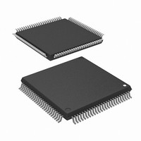
R5F2L3AAANFP#U1 Renesas Electronics America, R5F2L3AAANFP#U1 Datasheet - Page 213

R5F2L3AAANFP#U1
Manufacturer Part Number
R5F2L3AAANFP#U1
Description
MCU FLASH 96+4KB 100LQFP
Manufacturer
Renesas Electronics America
Series
R8C/Lx/3AAr
Datasheet
1.R5F2L387ANFPU1.pdf
(864 pages)
Specifications of R5F2L3AAANFP#U1
Core Processor
R8C
Core Size
16/32-Bit
Speed
20MHz
Connectivity
I²C, LIN, SIO, SSU, UART/USART
Peripherals
LCD, POR, PWM, Voltage Detect, WDT
Number Of I /o
88
Program Memory Size
96KB (96K x 8)
Program Memory Type
FLASH
Ram Size
10K x 8
Voltage - Supply (vcc/vdd)
1.8 V ~ 5.5 V
Data Converters
A/D 20x10b; D/A 2x8b
Oscillator Type
Internal
Operating Temperature
-20°C ~ 85°C
Package / Case
100-LQFP
Lead Free Status / RoHS Status
Lead free / RoHS Compliant
Eeprom Size
-
Available stocks
Company
Part Number
Manufacturer
Quantity
Price
- Current page: 213 of 864
- Download datasheet (16Mb)
R8C/L35A Group, R8C/L36A Group, R8C/L38A Group, R8C/L3AA Group,
R8C/L35B Group, R8C/L36B Group, R8C/L38B Group, R8C/L3AB Group
REJ09B0441-0100 Rev.1.00
Page 176 of 802
11.7
Figure 11.12
Table 11.10
Timer RC
Timer RD
Timer RG
Synchronous serial
communication unit
I
Flash memory
2
The interrupts of timer RC, timer RD (timer RD0) interrupt, timer RD (timer RD1), timer RG, the synchronous
serial communication unit, the I
sources. An interrupt request is generated by the logical OR of several interrupt request sources and is reflected in
the IR bit in the corresponding interrupt control register. Therefore, each of these peripheral functions has its own
interrupt request source status register (status register) and interrupt request source enable register (enable register)
to control the generation of interrupt requests (change of the IR bit in the interrupt control register). Table 11.10
lists the Registers Associated with Interrupts of Timer RC, Timer RD, Timer RG, Synchronous Serial
Communication Unit, I
Interrupt.
C bus interface
Peripheral Function
Interrupts of Timer RC, Timer RD, Timer RG, Synchronous Serial Communication
Unit, I
Request Sources)
Name
Timer RD0
Timer RD1
Registers Associated with Interrupts of Timer RC, Timer RD, Timer RG, Synchronous
Serial Communication Unit, I
Block Diagram of Timer RD Interrupt
2
i = 0 or 1
IMFA, IMFB, IMFC, IMFD, OVF, UDF: Bits in TRDSRi register
IMIEA, IMIEB, IMIEC, IMIED, OVIE: Bits in TRDIERi register
C bus Interface, and Flash Memory (Interrupts with Multiple Interrupt
OVIE bit
2
UDF bit
OVF bit
C bus Interface, and Flash Memory and Figure 11.12 shows a Block Diagram of Timer RD
Timer RDi
TRCSR
TRDSR0
TRDSR1
TRGSR
SSSR
ICSR
RDYSTI
BSYAEI
Interrupt Request Source
Oct 30, 2009
IMIEA bit
IMIEB bit
IMIEC bit
IMIED bit
IMFA bit
IMFB bit
IMFC bit
IMFD bit
Status Register of
2
C bus interface, and the flash memory each have multiple interrupt request
2
C bus Interface, and Flash Memory
Interrupt Request Source
TRCIER
TRDIER0
TRDIER1
TRGIER
SSER
ICIER
RDYSTIE
BSYAEIE
CMDERIE
Enable Register of
Timer RDi interrupt request
(IR bit in TRDiIC register)
TRD0IC
TRD1IC
TRCIC
TRGIC
SSUIC
IICIC
FMRDYIC
Interrupt Control
Register
11. Interrupts
Related parts for R5F2L3AAANFP#U1
Image
Part Number
Description
Manufacturer
Datasheet
Request
R

Part Number:
Description:
KIT STARTER FOR M16C/29
Manufacturer:
Renesas Electronics America
Datasheet:

Part Number:
Description:
KIT STARTER FOR R8C/2D
Manufacturer:
Renesas Electronics America
Datasheet:

Part Number:
Description:
R0K33062P STARTER KIT
Manufacturer:
Renesas Electronics America
Datasheet:

Part Number:
Description:
KIT STARTER FOR R8C/23 E8A
Manufacturer:
Renesas Electronics America
Datasheet:

Part Number:
Description:
KIT STARTER FOR R8C/25
Manufacturer:
Renesas Electronics America
Datasheet:

Part Number:
Description:
KIT STARTER H8S2456 SHARPE DSPLY
Manufacturer:
Renesas Electronics America
Datasheet:

Part Number:
Description:
KIT STARTER FOR R8C38C
Manufacturer:
Renesas Electronics America
Datasheet:

Part Number:
Description:
KIT STARTER FOR R8C35C
Manufacturer:
Renesas Electronics America
Datasheet:

Part Number:
Description:
KIT STARTER FOR R8CL3AC+LCD APPS
Manufacturer:
Renesas Electronics America
Datasheet:

Part Number:
Description:
KIT STARTER FOR RX610
Manufacturer:
Renesas Electronics America
Datasheet:

Part Number:
Description:
KIT STARTER FOR R32C/118
Manufacturer:
Renesas Electronics America
Datasheet:

Part Number:
Description:
KIT DEV RSK-R8C/26-29
Manufacturer:
Renesas Electronics America
Datasheet:

Part Number:
Description:
KIT STARTER FOR SH7124
Manufacturer:
Renesas Electronics America
Datasheet:

Part Number:
Description:
KIT STARTER FOR H8SX/1622
Manufacturer:
Renesas Electronics America
Datasheet:

Part Number:
Description:
KIT DEV FOR SH7203
Manufacturer:
Renesas Electronics America
Datasheet:


