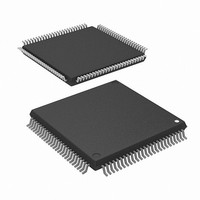
R5F2L3AAANFP#U1 Renesas Electronics America, R5F2L3AAANFP#U1 Datasheet - Page 772

R5F2L3AAANFP#U1
Manufacturer Part Number
R5F2L3AAANFP#U1
Description
MCU FLASH 96+4KB 100LQFP
Manufacturer
Renesas Electronics America
Series
R8C/Lx/3AAr
Datasheet
1.R5F2L387ANFPU1.pdf
(864 pages)
Specifications of R5F2L3AAANFP#U1
Core Processor
R8C
Core Size
16/32-Bit
Speed
20MHz
Connectivity
I²C, LIN, SIO, SSU, UART/USART
Peripherals
LCD, POR, PWM, Voltage Detect, WDT
Number Of I /o
88
Program Memory Size
96KB (96K x 8)
Program Memory Type
FLASH
Ram Size
10K x 8
Voltage - Supply (vcc/vdd)
1.8 V ~ 5.5 V
Data Converters
A/D 20x10b; D/A 2x8b
Oscillator Type
Internal
Operating Temperature
-20°C ~ 85°C
Package / Case
100-LQFP
Lead Free Status / RoHS Status
Lead free / RoHS Compliant
Eeprom Size
-
Available stocks
Company
Part Number
Manufacturer
Quantity
Price
- Current page: 772 of 864
- Download datasheet (16Mb)
R8C/L35A Group, R8C/L36A Group, R8C/L38A Group, R8C/L3AA Group,
R8C/L35B Group, R8C/L36B Group, R8C/L38B Group, R8C/L3AB Group
REJ09B0441-0100 Rev.1.00
Page 735 of 802
Figure 34.2
Table 34.7
Notes:
t
d(SR-SUS)
Symbol
1. Definition of programming/erasure endurance
2. Endurance to guarantee all electrical characteristics after program and erase. (1 to Min. value can be guaranteed).
3. In a system that executes multiple programming operations, the actual erasure count can be reduced by writing to sequential
4. If an error occurs during block erase, attempt to execute the clear status register command, then execute the block erase
5. Customers desiring program/erase failure rate information should contact their Renesas technical support representative.
6.
7.
The programming and erasure endurance is defined on a per-block basis.
If the programming and erasure endurance is n (n = 10,000), each block can be erased n times. For example, if 1,024 1-byte
writes are performed to different addresses in block A, a 1 Kbyte block, and then the block is erased, the
programming/erasure endurance still stands at one.
However, the same address must not be programmed more than once per erase operation (overwriting prohibited).
addresses in turn so that as much of the block as possible is used up before performing an erase operation. For example,
when programming groups of 16 bytes, the effective number of rewrites can be minimized by programming up to 128 groups
before erasing them all in one operation. In addition, averaging the erasure endurance between blocks A to D can further
reduce the actual erasure endurance. It is also advisable to retain data on the erasure endurance of each block and limit the
number of erase operations to a certain number.
command at least three times until the erase error does not occur.
The data hold time includes time that the power supply is off or the clock is not supplied.
40 C for D version.
Program/erase endurance
Byte program time
(program/erase endurance
Byte program time
(program/erase endurance
Block erase time
(program/erase endurance
Block erase time
(program/erase endurance
Time delay from suspend request until
suspend
Interval from erase start/restart until
following suspend request
Suspend interval necessary for auto-
erasure to complete
Time from suspend until erase restart
Program, erase voltage
Read voltage
Program, erase temperature
Data hold time
Suspend request
FST6: Bit in FST register
FMR21: Bit in FMR2 register
(V
otherwise specified.)
Time delay until Suspend
Flash Memory (Data flash Block A to Block D) Characteristics
CC
(FMR21 bit)
FST6 bit
= 2.7 to 5.5 V and T
(7)
Parameter
Oct 30, 2009
(1)
1,000 times)
1,000 times)
1,000 times)
1,000 times)
opr
= 20 to 85 C (N version) / 40 to 85 C (D version), unless
Ambient temperature = 55 C
Fixed time
Conditions
t
d(SR-SUS)
Clock-dependent
time
10,000
Min.
20
2.7
1.8
33
33
20
(6)
(2)
34. Electrical Characteristics
Access restart
Typ.
160
300
0.2
0.3
Standard
30 + CPU clock
5 + CPU clock
× 3 cycles
× 1 cycle
Max.
TBD
5.5
5.5
85
times
year
Unit
ms
ms
ms
V
V
s
s
C
s
s
s
Related parts for R5F2L3AAANFP#U1
Image
Part Number
Description
Manufacturer
Datasheet
Request
R

Part Number:
Description:
KIT STARTER FOR M16C/29
Manufacturer:
Renesas Electronics America
Datasheet:

Part Number:
Description:
KIT STARTER FOR R8C/2D
Manufacturer:
Renesas Electronics America
Datasheet:

Part Number:
Description:
R0K33062P STARTER KIT
Manufacturer:
Renesas Electronics America
Datasheet:

Part Number:
Description:
KIT STARTER FOR R8C/23 E8A
Manufacturer:
Renesas Electronics America
Datasheet:

Part Number:
Description:
KIT STARTER FOR R8C/25
Manufacturer:
Renesas Electronics America
Datasheet:

Part Number:
Description:
KIT STARTER H8S2456 SHARPE DSPLY
Manufacturer:
Renesas Electronics America
Datasheet:

Part Number:
Description:
KIT STARTER FOR R8C38C
Manufacturer:
Renesas Electronics America
Datasheet:

Part Number:
Description:
KIT STARTER FOR R8C35C
Manufacturer:
Renesas Electronics America
Datasheet:

Part Number:
Description:
KIT STARTER FOR R8CL3AC+LCD APPS
Manufacturer:
Renesas Electronics America
Datasheet:

Part Number:
Description:
KIT STARTER FOR RX610
Manufacturer:
Renesas Electronics America
Datasheet:

Part Number:
Description:
KIT STARTER FOR R32C/118
Manufacturer:
Renesas Electronics America
Datasheet:

Part Number:
Description:
KIT DEV RSK-R8C/26-29
Manufacturer:
Renesas Electronics America
Datasheet:

Part Number:
Description:
KIT STARTER FOR SH7124
Manufacturer:
Renesas Electronics America
Datasheet:

Part Number:
Description:
KIT STARTER FOR H8SX/1622
Manufacturer:
Renesas Electronics America
Datasheet:

Part Number:
Description:
KIT DEV FOR SH7203
Manufacturer:
Renesas Electronics America
Datasheet:


