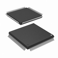
R5F2L3AAANFP#U1 Renesas Electronics America, R5F2L3AAANFP#U1 Datasheet - Page 177

R5F2L3AAANFP#U1
Manufacturer Part Number
R5F2L3AAANFP#U1
Description
MCU FLASH 96+4KB 100LQFP
Manufacturer
Renesas Electronics America
Series
R8C/Lx/3AAr
Datasheet
1.R5F2L387ANFPU1.pdf
(864 pages)
Specifications of R5F2L3AAANFP#U1
Core Processor
R8C
Core Size
16/32-Bit
Speed
20MHz
Connectivity
I²C, LIN, SIO, SSU, UART/USART
Peripherals
LCD, POR, PWM, Voltage Detect, WDT
Number Of I /o
88
Program Memory Size
96KB (96K x 8)
Program Memory Type
FLASH
Ram Size
10K x 8
Voltage - Supply (vcc/vdd)
1.8 V ~ 5.5 V
Data Converters
A/D 20x10b; D/A 2x8b
Oscillator Type
Internal
Operating Temperature
-20°C ~ 85°C
Package / Case
100-LQFP
Lead Free Status / RoHS Status
Lead free / RoHS Compliant
Eeprom Size
-
Available stocks
Company
Part Number
Manufacturer
Quantity
Price
- Current page: 177 of 864
- Download datasheet (16Mb)
R8C/L35A Group, R8C/L36A Group, R8C/L38A Group, R8C/L3AA Group,
R8C/L35B Group, R8C/L36B Group, R8C/L38B Group, R8C/L3AB Group
REJ09B0441-0100 Rev.1.00
Page 140 of 802
Figure 9.6
9.6.4
Table 9.5
Notes:
Table 9.6
Write the pin state and the exit
method to the POMCR0 register
in power-off mode.
Then, write 88h,15h, 92h, and 25h
successively.
Ports P0 to P7
Ports 10 to P13
WKUP0
XCIN, XCOUT
VL1 to VL4
1. To use WKUP1 to exit power-off mode, set the POM03 bit to 1 (input enabled) by the initial write to the
2. To use timer RE to exit power-off mode, enable the timer RE interrupt in registers TREIC and TRECR2, then
To exit power-off mode, input a low signal pulse to the RESET, WKUP0, or WKUP1 pin or use the timer RE
interrupt (power-off 1 is selected). The timer RE interrupt enabled in the TREC2 register can be used to exit the
mode.
After exiting power-off mode, the operation is the same as a normal reset sequence.
When power-off mode is exited, the exit source can be identified by reading the flags in the SDCR0 register.
The values of these flags are undefined after power-on and set to 0 by writing to the SDCR0 register. If multiple
exit sources coincide, multiple flags are set.
Figure 9.6 show the Time from Power-Off Mode to Reset Vector Address Read Execution.
Stabilization Time (T0)
Note:
Entering Power-Off Mode
POMCR0 register. The WKUP1 pin is not available in the R8C/L35A, R8C/L35B, R8C/L36A, and R8C/L36B
Groups.
set the POM00 bit in the POMCR0 register to 1 (timer RE enabled). When all interrupts are disabled by the
TRECR2 register, the low-speed clock and timer RE functions operate, but timer RE cannot be used to exit
power-off mode.
Pin Name
1. If the low-level input width of the RESET, WKUP0, or WKUP1 pin exceeds the internal power stabilization time and internal reset time
Internal Power
Power-off mode
Max. 2 ms
(T0 + T1), the excess is added to the time until a reset vector address is read. (The low-level input width of the RESET, WKUP0, or
WKUP1 pin requires 10 s or more).
Exiting Power-Off Mode
Pin Status in Power-Off Mode
Entering Power-Off Mode and Exit Methods
Time from Power-Off Mode to Reset Vector Address Read Execution
(fOCO-S clock
Internal Reset Time (T1)
Power-off exit source generation
The states of registers LSE0 to LSE7 before entering power-off mode are retained. When
LCD ports are selected by these registers, low-level output. When ports are selected, the
pins are placed in the high-impedance state.
High impedance
WKUP0 input
Oscillation is off (high impedance) at power-off 0, and oscillation is on at power-off 1.
High impedance
stabilization time
Internal power
Oct 30, 2009
T0
64 s
(1, 2)
8 cycles)
All functions stop when the SDC00 bit is
set to 0 (power-off 0) by the initial write.
Functions other the low-speed clock and
timer RE stop when the SDC00 bit is set to
1 (power-off 1) by the initial write.
Internal reset time
CPU clock
Flash Memory Activation (T2)
T1
Max. 1,424 s
Time until
108 to 178 cycles
Status
activation sequence
Flash memory
Status
CPU clock
T2
Idling Time (T3)
224 s
28 cycles
RESET input, WKUP0 input, or
WKUP1 input
RESET input, timer RE interrupt,
WKUP0 input, or WKUP1 input
The total of T0 to T3 is
the time from power-off mode
until a reset vector address is
read.
Idling time
T3
Exit Method
Remarks
9. Power Control
Related parts for R5F2L3AAANFP#U1
Image
Part Number
Description
Manufacturer
Datasheet
Request
R

Part Number:
Description:
KIT STARTER FOR M16C/29
Manufacturer:
Renesas Electronics America
Datasheet:

Part Number:
Description:
KIT STARTER FOR R8C/2D
Manufacturer:
Renesas Electronics America
Datasheet:

Part Number:
Description:
R0K33062P STARTER KIT
Manufacturer:
Renesas Electronics America
Datasheet:

Part Number:
Description:
KIT STARTER FOR R8C/23 E8A
Manufacturer:
Renesas Electronics America
Datasheet:

Part Number:
Description:
KIT STARTER FOR R8C/25
Manufacturer:
Renesas Electronics America
Datasheet:

Part Number:
Description:
KIT STARTER H8S2456 SHARPE DSPLY
Manufacturer:
Renesas Electronics America
Datasheet:

Part Number:
Description:
KIT STARTER FOR R8C38C
Manufacturer:
Renesas Electronics America
Datasheet:

Part Number:
Description:
KIT STARTER FOR R8C35C
Manufacturer:
Renesas Electronics America
Datasheet:

Part Number:
Description:
KIT STARTER FOR R8CL3AC+LCD APPS
Manufacturer:
Renesas Electronics America
Datasheet:

Part Number:
Description:
KIT STARTER FOR RX610
Manufacturer:
Renesas Electronics America
Datasheet:

Part Number:
Description:
KIT STARTER FOR R32C/118
Manufacturer:
Renesas Electronics America
Datasheet:

Part Number:
Description:
KIT DEV RSK-R8C/26-29
Manufacturer:
Renesas Electronics America
Datasheet:

Part Number:
Description:
KIT STARTER FOR SH7124
Manufacturer:
Renesas Electronics America
Datasheet:

Part Number:
Description:
KIT STARTER FOR H8SX/1622
Manufacturer:
Renesas Electronics America
Datasheet:

Part Number:
Description:
KIT DEV FOR SH7203
Manufacturer:
Renesas Electronics America
Datasheet:


