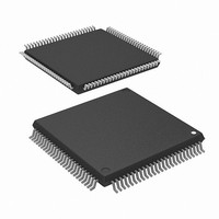
R5F2L3AAANFP#U1 Renesas Electronics America, R5F2L3AAANFP#U1 Datasheet - Page 677

R5F2L3AAANFP#U1
Manufacturer Part Number
R5F2L3AAANFP#U1
Description
MCU FLASH 96+4KB 100LQFP
Manufacturer
Renesas Electronics America
Series
R8C/Lx/3AAr
Datasheet
1.R5F2L387ANFPU1.pdf
(864 pages)
Specifications of R5F2L3AAANFP#U1
Core Processor
R8C
Core Size
16/32-Bit
Speed
20MHz
Connectivity
I²C, LIN, SIO, SSU, UART/USART
Peripherals
LCD, POR, PWM, Voltage Detect, WDT
Number Of I /o
88
Program Memory Size
96KB (96K x 8)
Program Memory Type
FLASH
Ram Size
10K x 8
Voltage - Supply (vcc/vdd)
1.8 V ~ 5.5 V
Data Converters
A/D 20x10b; D/A 2x8b
Oscillator Type
Internal
Operating Temperature
-20°C ~ 85°C
Package / Case
100-LQFP
Lead Free Status / RoHS Status
Lead free / RoHS Compliant
Eeprom Size
-
Available stocks
Company
Part Number
Manufacturer
Quantity
Price
- Current page: 677 of 864
- Download datasheet (16Mb)
R8C/L35A Group, R8C/L36A Group, R8C/L38A Group, R8C/L3AA Group,
R8C/L35B Group, R8C/L36B Group, R8C/L38B Group, R8C/L3AB Group
REJ09B0441-0100 Rev.1.00
Page 640 of 802
29.3.4
29.3.5
29.3.6
29.3.7
The A/D conversion result is stored in the ADi register (i = 0 to 7). The register where the result is stored varies
depending on the A/D operating mode used. The contents of the ADi register are undefined after reset. Values
cannot be written to the ADi register.
In repeat mode 0, no interrupt request is generated. After the first AD conversion is completed, determine if the
A/D conversion time has elapsed by a program.
In one-shot mode, repeat mode 1, single sweep mode, and repeat sweep mode, an interrupt request is generated
at certain times, such as when an A/D conversion completes (the IR bit in the ADIC register is set to 1).
However, in repeat mode 1 and repeat sweep mode, A/D conversion continues after an interrupt request is
generated. Read the ADi register before the next A/D conversion is completed, since at completion the ADi
register is rewritten with the new value.
In one-shot mode and single sweep mode, when bits ADCAP1 to ADCAP0 in the ADMOD register is set to
00b (software trigger), the ADST bit in the ADCON0 register is used to determine whether the A/D conversion
or sweep has completed.
During an A/D conversion operation, if the ADST bit in the ADCON0 register is set to 0 (A/D conversion
stops) by a program to forcibly terminate A/D conversion, the conversion result of the A/D converter is
undefined and no interrupt is generated. The value of the ADi register before A/D conversion may also be
undefined.
If the ADST bit is set to 0 by a program, do not use the value of all the ADi register.
When the A/D converter is not used, power consumption can be reduced by setting the ADSTBY bit in the
ADCON1 register to 0 (A/D operation stops (standby)) to shut off any analog circuit current flow.
To use the A/D converter, set the ADSTBY bit to 1 (A/D operation enabled) and wait for one AD cycle or
more before setting the ADST bit in the ADCON0 register to 1 (A/D conversion starts). Do not write 1 to bits
ADST and ADSTBY at the same time.
Also, do not set the ADSTBY bit to 0 (A/D operation stops (standby)) during the A/D conversion.
In one-shot mode, repeat mode 0, and repeat mode 1, the on-chip reference voltage (OCVREF) can be used as
analog input.
Any variation in VREF can be confirmed using the on-chip reference voltage. Use the ADEX0 bit in the
ADCON1 register and the OCVREFAN bit in the OCVREFCR register to select the on-chip reference voltage.
The A/D conversion result of the on-chip reference voltage in one-shot mode or in repeat mode 0 is stored in the
AD0 register.
To suppress influences of the analog input voltage leakage from the previously converted channel during A/D
conversion operation, a function is incorporated to fix the electric charge on the chopper amp capacitor to the
predetermined state (AVCC or GND) before starting conversion.
This function enables more reliable detection of an open circuit in the wiring connected to the analog input pins.
Figure 29.5 shows the A/D Open-Circuit Detection Example on AVCC Side (Precharge before Conversion
Selected) and Figure 29.6 shows the A/D Open-Circuit Detection Example on AVSS Side (Discharge before
Conversion Selected).
A/D Conversion Result
Low-Current-Consumption Function
Extended Analog Input Pins
A/D Open-Circuit Detection Assist Function
Oct 30, 2009
29. A/D Converter
Related parts for R5F2L3AAANFP#U1
Image
Part Number
Description
Manufacturer
Datasheet
Request
R

Part Number:
Description:
KIT STARTER FOR M16C/29
Manufacturer:
Renesas Electronics America
Datasheet:

Part Number:
Description:
KIT STARTER FOR R8C/2D
Manufacturer:
Renesas Electronics America
Datasheet:

Part Number:
Description:
R0K33062P STARTER KIT
Manufacturer:
Renesas Electronics America
Datasheet:

Part Number:
Description:
KIT STARTER FOR R8C/23 E8A
Manufacturer:
Renesas Electronics America
Datasheet:

Part Number:
Description:
KIT STARTER FOR R8C/25
Manufacturer:
Renesas Electronics America
Datasheet:

Part Number:
Description:
KIT STARTER H8S2456 SHARPE DSPLY
Manufacturer:
Renesas Electronics America
Datasheet:

Part Number:
Description:
KIT STARTER FOR R8C38C
Manufacturer:
Renesas Electronics America
Datasheet:

Part Number:
Description:
KIT STARTER FOR R8C35C
Manufacturer:
Renesas Electronics America
Datasheet:

Part Number:
Description:
KIT STARTER FOR R8CL3AC+LCD APPS
Manufacturer:
Renesas Electronics America
Datasheet:

Part Number:
Description:
KIT STARTER FOR RX610
Manufacturer:
Renesas Electronics America
Datasheet:

Part Number:
Description:
KIT STARTER FOR R32C/118
Manufacturer:
Renesas Electronics America
Datasheet:

Part Number:
Description:
KIT DEV RSK-R8C/26-29
Manufacturer:
Renesas Electronics America
Datasheet:

Part Number:
Description:
KIT STARTER FOR SH7124
Manufacturer:
Renesas Electronics America
Datasheet:

Part Number:
Description:
KIT STARTER FOR H8SX/1622
Manufacturer:
Renesas Electronics America
Datasheet:

Part Number:
Description:
KIT DEV FOR SH7203
Manufacturer:
Renesas Electronics America
Datasheet:


