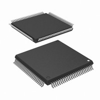
R5F2L3AAANFP#U1 Renesas Electronics America, R5F2L3AAANFP#U1 Datasheet - Page 490

R5F2L3AAANFP#U1
Manufacturer Part Number
R5F2L3AAANFP#U1
Description
MCU FLASH 96+4KB 100LQFP
Manufacturer
Renesas Electronics America
Series
R8C/Lx/3AAr
Datasheet
1.R5F2L387ANFPU1.pdf
(864 pages)
Specifications of R5F2L3AAANFP#U1
Core Processor
R8C
Core Size
16/32-Bit
Speed
20MHz
Connectivity
I²C, LIN, SIO, SSU, UART/USART
Peripherals
LCD, POR, PWM, Voltage Detect, WDT
Number Of I /o
88
Program Memory Size
96KB (96K x 8)
Program Memory Type
FLASH
Ram Size
10K x 8
Voltage - Supply (vcc/vdd)
1.8 V ~ 5.5 V
Data Converters
A/D 20x10b; D/A 2x8b
Oscillator Type
Internal
Operating Temperature
-20°C ~ 85°C
Package / Case
100-LQFP
Lead Free Status / RoHS Status
Lead free / RoHS Compliant
Eeprom Size
-
Available stocks
Company
Part Number
Manufacturer
Quantity
Price
- Current page: 490 of 864
- Download datasheet (16Mb)
R8C/L35A Group, R8C/L36A Group, R8C/L38A Group, R8C/L3AA Group,
R8C/L35B Group, R8C/L36B Group, R8C/L38B Group, R8C/L3AB Group
REJ09B0441-0100 Rev.1.00
Page 453 of 802
22.2.8
After Reset
After Reset
b15 to b0 Function varies depending on the operating mode.
Address 0179h to 0178h (TRGGRA), 017Bh to 017Ah (TRGGRB),
Symbol
Symbol
Bit
TRGGRA and TRGGRB are 16-bit readable/writable registers with both the output compare and input capture
register functions. Switching between these functions is accomplished by means of a setting in the TRGIOR
register.
When registers TRGGRA and TRGGRB are used as output compare registers, the values of registers TRGGRA
and TRGGRB and the value of the TRG register are always compared. When their values match (compare
match), bits IMFA and IMFB in the TRGSR register are set to 1. Compare match output can be selected by
setting the TRGIOR register.
When registers TRGGRA and TRGGRB are used as input capture registers, the value of the TRG register is
stored when an externally input capture signals is detected. Bits IMFA and IMFB in the TRGSR register are set
to 1 at this time. The detection edge of input capture signals is selected by setting the TRGIOR register.
In PWM mode, the settings of the TRGIOR register are ignored.
The TRGGRC register can also be used as the buffer register of the TRGGRA register, and the TRGGRD
register can be used as the buffer register of the TRGGRB register, respectively. These functions can be
selected by setting bits BUFA and BUFB in the TRGIOR register.
For example, when the TRGGRA register is set as an output compare register and the TRGGRC register is set
as the buffer register of the TRGGRA register, the value of the TRGGRC register is transferred to the
TRGGRA register each time compare match A occurs.
When the TRGGRA register is set as an input capture register and the TRGGRC register is set as the buffer
register of the TRGGRA register, the value of the TRG register is transferred to the TRGGRA register and the
value of the TRGGRA register value is transferred to the TRGGRC register each time an input capture occurs.
Registers TRGGRA and TRGGRB are connected to the CPU via the internal 16-bit bus and should be accessed
in 16-bit units. These registers are set as output compare registers (pin output disabled) after a reset.
Bit
Bit
Timer RG General Register A, B, C, D (TRGGRA, TRGGRB, TRGGRC,
TRGGRD)
017Dh to 017Ch (TRGGRC), 017Fh to 017Eh (TRGGRD)
b15
b7
—
—
1
1
b14
b6
—
—
1
1
Oct 30, 2009
b13
b5
—
—
1
1
b12
b4
—
—
1
1
Function
b11
b3
—
—
1
1
b10
b2
—
—
1
1
b1
b9
—
—
1
1
b0
b8
—
—
1
1
22. Timer RG
R/W
R/W
Related parts for R5F2L3AAANFP#U1
Image
Part Number
Description
Manufacturer
Datasheet
Request
R

Part Number:
Description:
KIT STARTER FOR M16C/29
Manufacturer:
Renesas Electronics America
Datasheet:

Part Number:
Description:
KIT STARTER FOR R8C/2D
Manufacturer:
Renesas Electronics America
Datasheet:

Part Number:
Description:
R0K33062P STARTER KIT
Manufacturer:
Renesas Electronics America
Datasheet:

Part Number:
Description:
KIT STARTER FOR R8C/23 E8A
Manufacturer:
Renesas Electronics America
Datasheet:

Part Number:
Description:
KIT STARTER FOR R8C/25
Manufacturer:
Renesas Electronics America
Datasheet:

Part Number:
Description:
KIT STARTER H8S2456 SHARPE DSPLY
Manufacturer:
Renesas Electronics America
Datasheet:

Part Number:
Description:
KIT STARTER FOR R8C38C
Manufacturer:
Renesas Electronics America
Datasheet:

Part Number:
Description:
KIT STARTER FOR R8C35C
Manufacturer:
Renesas Electronics America
Datasheet:

Part Number:
Description:
KIT STARTER FOR R8CL3AC+LCD APPS
Manufacturer:
Renesas Electronics America
Datasheet:

Part Number:
Description:
KIT STARTER FOR RX610
Manufacturer:
Renesas Electronics America
Datasheet:

Part Number:
Description:
KIT STARTER FOR R32C/118
Manufacturer:
Renesas Electronics America
Datasheet:

Part Number:
Description:
KIT DEV RSK-R8C/26-29
Manufacturer:
Renesas Electronics America
Datasheet:

Part Number:
Description:
KIT STARTER FOR SH7124
Manufacturer:
Renesas Electronics America
Datasheet:

Part Number:
Description:
KIT STARTER FOR H8SX/1622
Manufacturer:
Renesas Electronics America
Datasheet:

Part Number:
Description:
KIT DEV FOR SH7203
Manufacturer:
Renesas Electronics America
Datasheet:


