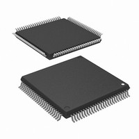
R5F2L3AAANFP#U1 Renesas Electronics America, R5F2L3AAANFP#U1 Datasheet - Page 645

R5F2L3AAANFP#U1
Manufacturer Part Number
R5F2L3AAANFP#U1
Description
MCU FLASH 96+4KB 100LQFP
Manufacturer
Renesas Electronics America
Series
R8C/Lx/3AAr
Datasheet
1.R5F2L387ANFPU1.pdf
(864 pages)
Specifications of R5F2L3AAANFP#U1
Core Processor
R8C
Core Size
16/32-Bit
Speed
20MHz
Connectivity
I²C, LIN, SIO, SSU, UART/USART
Peripherals
LCD, POR, PWM, Voltage Detect, WDT
Number Of I /o
88
Program Memory Size
96KB (96K x 8)
Program Memory Type
FLASH
Ram Size
10K x 8
Voltage - Supply (vcc/vdd)
1.8 V ~ 5.5 V
Data Converters
A/D 20x10b; D/A 2x8b
Oscillator Type
Internal
Operating Temperature
-20°C ~ 85°C
Package / Case
100-LQFP
Lead Free Status / RoHS Status
Lead free / RoHS Compliant
Eeprom Size
-
Available stocks
Company
Part Number
Manufacturer
Quantity
Price
- Current page: 645 of 864
- Download datasheet (16Mb)
R8C/L35A Group, R8C/L36A Group, R8C/L38A Group, R8C/L3AA Group,
R8C/L35B Group, R8C/L36B Group, R8C/L38B Group, R8C/L3AB Group
REJ09B0441-0100 Rev.1.00
Page 608 of 802
27.6
Figure 27.16
Figures 27.16 to 27.19 show Register Setting Examples When Using I
Register Setting Examples
Register Setting Example in Master Transmit Mode (I
Read the ACKBR bit in the ICIER register
ICCR1 register
ICCR2 register
Write transmit data to the ICDRT register
Write transmit data to the ICDRT register
Write transmit data to the ICDRT register
ICSR register
ICSR register
ICCR2 register
ICCR1 register
ICSR register
Read the BBSY bit in the ICCR2 register
Read the TEND bit in the ICSR register
Read the TDRE bit in the ICSR register
Read the TEND bit in the ICSR register
Read the STOP bit in the ICSR register
No
No
No
No
No
No
Oct 30, 2009
Initial setting
ACKBR = 0?
Yes
BBSY = 0?
TEND = 1?
TDRE = 1?
TEND = 1?
Last byte?
STOP = 1?
TDRE bit
Transmit
mode?
TEND bit
TRS bit
MST bit
SCP bit
BBSY bit
SCP bit
BBSY bit
TRS bit
MST bit
STOP bit
Start
End
Yes
Yes
Yes
Yes
Yes
Yes
Yes
1
0
0
0
1
0
0
0
1
0
0
No
No
(1)
(2)
(3)
(4)
(5)
(6)
(7)
(8)
(9)
(10)
(11)
(12)
(13)
(14)
(15)
Master receive mode
• Set the STOP bit in the ICSR register to 0.
• Set the IICSEL bit in the SSUIICSR register to 1.
• Set the MSTIIC bit in the MSTCR register to 0.
(1) Determine the states of the SCL and SDA lines.
(2) Set to master transmit mode.
(3) Generate a start condition.
(4) Set the transmit data of the 1st byte
(5) Wait until 1 byte of data is transmitted.
(6) Determine the ACKBR bit from the specified
(7) Set the transmit data after 2nd byte
(8) Wait until the ICRDT register is empty.
(9) Set the transmit data of the last byte.
(10) Wait until the last byte is transmitted.
(11) Set the TEND bit to 0.
(12) Set the STOP bit to 0.
(13) Generate a stop condition.
(14) Wait until a stop condition is generated.
(15) Set to slave receive mode.
(slave address + R/W).
slave device.
(except the last byte).
Set the TDRE bit to 0.
2
C bus interface.
2
C bus Interface Mode)
27. I
2
C bus Interface
Related parts for R5F2L3AAANFP#U1
Image
Part Number
Description
Manufacturer
Datasheet
Request
R

Part Number:
Description:
KIT STARTER FOR M16C/29
Manufacturer:
Renesas Electronics America
Datasheet:

Part Number:
Description:
KIT STARTER FOR R8C/2D
Manufacturer:
Renesas Electronics America
Datasheet:

Part Number:
Description:
R0K33062P STARTER KIT
Manufacturer:
Renesas Electronics America
Datasheet:

Part Number:
Description:
KIT STARTER FOR R8C/23 E8A
Manufacturer:
Renesas Electronics America
Datasheet:

Part Number:
Description:
KIT STARTER FOR R8C/25
Manufacturer:
Renesas Electronics America
Datasheet:

Part Number:
Description:
KIT STARTER H8S2456 SHARPE DSPLY
Manufacturer:
Renesas Electronics America
Datasheet:

Part Number:
Description:
KIT STARTER FOR R8C38C
Manufacturer:
Renesas Electronics America
Datasheet:

Part Number:
Description:
KIT STARTER FOR R8C35C
Manufacturer:
Renesas Electronics America
Datasheet:

Part Number:
Description:
KIT STARTER FOR R8CL3AC+LCD APPS
Manufacturer:
Renesas Electronics America
Datasheet:

Part Number:
Description:
KIT STARTER FOR RX610
Manufacturer:
Renesas Electronics America
Datasheet:

Part Number:
Description:
KIT STARTER FOR R32C/118
Manufacturer:
Renesas Electronics America
Datasheet:

Part Number:
Description:
KIT DEV RSK-R8C/26-29
Manufacturer:
Renesas Electronics America
Datasheet:

Part Number:
Description:
KIT STARTER FOR SH7124
Manufacturer:
Renesas Electronics America
Datasheet:

Part Number:
Description:
KIT STARTER FOR H8SX/1622
Manufacturer:
Renesas Electronics America
Datasheet:

Part Number:
Description:
KIT DEV FOR SH7203
Manufacturer:
Renesas Electronics America
Datasheet:


