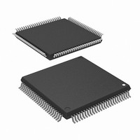
R5F2L3AAANFP#U1 Renesas Electronics America, R5F2L3AAANFP#U1 Datasheet - Page 851

R5F2L3AAANFP#U1
Manufacturer Part Number
R5F2L3AAANFP#U1
Description
MCU FLASH 96+4KB 100LQFP
Manufacturer
Renesas Electronics America
Series
R8C/Lx/3AAr
Datasheet
1.R5F2L387ANFPU1.pdf
(864 pages)
Specifications of R5F2L3AAANFP#U1
Core Processor
R8C
Core Size
16/32-Bit
Speed
20MHz
Connectivity
I²C, LIN, SIO, SSU, UART/USART
Peripherals
LCD, POR, PWM, Voltage Detect, WDT
Number Of I /o
88
Program Memory Size
96KB (96K x 8)
Program Memory Type
FLASH
Ram Size
10K x 8
Voltage - Supply (vcc/vdd)
1.8 V ~ 5.5 V
Data Converters
A/D 20x10b; D/A 2x8b
Oscillator Type
Internal
Operating Temperature
-20°C ~ 85°C
Package / Case
100-LQFP
Lead Free Status / RoHS Status
Lead free / RoHS Compliant
Eeprom Size
-
Available stocks
Company
Part Number
Manufacturer
Quantity
Price
- Current page: 851 of 864
- Download datasheet (16Mb)
1.00
Rev.
REVISION HISTORY
Oct 30, 2009
Date
236, 758 17.8, 35.7 “In pulse period measurement mode,...”
Page
203
207
214
215
219
220
222
224
226
228
229
230
233
237
245
250
251
257
258
262
272
275
278
279
283
285
15.2.8 revised
Table 15.5 “Voltage detection circuit” deleted
15.3.8 “four clock”
Table 15.9 revised, Note 2 added
Table 15.10 “J: Number of cycles required to read or write back control
data”
number of cycles required to write back control data”
Table 16.1 “Count sources” revised
Figure 17.1 revised
17.2.3 b4 to b6 “fOCO”
Table 17.2 “fOCO”
Table 17.3 “fOCO”
Table 17.4 Selectable functions INT2
17.5.1 b6 to b7 revised
Table 17.5 “fOCO”
Table 17.6 “fOCO”
measurement mode and pulse period measurement mode,...”
Figure 18.1 revised
Table 18.3 Selectable function Waveform output enable/disable function,
Note 3, added
Figure 18.4 revised
18.5.3
“ Set the INT0EN bit in the INTEN register to 0 (enabled).”
“ After completing the above, ... (INT pin ...”
19.1 “Timer RC uses either f1, fOCO40M or fOCO-F as its operating
clock.” “Timer RC uses f1 as its operating clock.”
Table 19.1 revised
Figure 19.1 “fOCO40M, fOCO-F” deleted
19.2.3 b4 to b6 revised, Note 2 deleted
Table 19.5 “fOCO40M”, “fOCO-F” deleted
Figure 19.2 “fOCO40M”, “fOCO-F” deleted
“To select fOCO40M or fOCO-F as the count source,...in the TRCCR1
register to 110b (fOCO40M) or 111b (fOCO-F).” deleted
Figure 19.5 “fOCO40M”, “fOCO-F” deleted
Table 19.7 “fOCO40M, fOCO-F” deleted
Figure 19.7 revised
Table 19.9 “fOCO40M, fOCO-F” deleted
19.5.1 b4 to b6 revised, Note 3 deleted
R8C/L35A Group, R8C/L35B Group, R8C/L36A Group, R8C/L36B Group, R8C/L38A Group,
R8C/L38B Group, R8C/L3AA Group, R8C/L3AB Group Hardware Manual
“ Set the INT0EN bit in the INTEN register to 1 (enabled).”
“ After completing the above, ... (INT0 pin ...”
“J: Number of cycles required to read control data (5 cycles) +
C - 12
“five clock”, Figure15.11, Figure 15.12 revised
“fOCO-S”
“fOCO-S”, Selectable functions revised
“fOCO-S”, Selectable functions revised
“fOCO-S”, Selectable functions revised
Description
“fOCO-S”
Summary
TRAIO
“In pulse width
Related parts for R5F2L3AAANFP#U1
Image
Part Number
Description
Manufacturer
Datasheet
Request
R

Part Number:
Description:
KIT STARTER FOR M16C/29
Manufacturer:
Renesas Electronics America
Datasheet:

Part Number:
Description:
KIT STARTER FOR R8C/2D
Manufacturer:
Renesas Electronics America
Datasheet:

Part Number:
Description:
R0K33062P STARTER KIT
Manufacturer:
Renesas Electronics America
Datasheet:

Part Number:
Description:
KIT STARTER FOR R8C/23 E8A
Manufacturer:
Renesas Electronics America
Datasheet:

Part Number:
Description:
KIT STARTER FOR R8C/25
Manufacturer:
Renesas Electronics America
Datasheet:

Part Number:
Description:
KIT STARTER H8S2456 SHARPE DSPLY
Manufacturer:
Renesas Electronics America
Datasheet:

Part Number:
Description:
KIT STARTER FOR R8C38C
Manufacturer:
Renesas Electronics America
Datasheet:

Part Number:
Description:
KIT STARTER FOR R8C35C
Manufacturer:
Renesas Electronics America
Datasheet:

Part Number:
Description:
KIT STARTER FOR R8CL3AC+LCD APPS
Manufacturer:
Renesas Electronics America
Datasheet:

Part Number:
Description:
KIT STARTER FOR RX610
Manufacturer:
Renesas Electronics America
Datasheet:

Part Number:
Description:
KIT STARTER FOR R32C/118
Manufacturer:
Renesas Electronics America
Datasheet:

Part Number:
Description:
KIT DEV RSK-R8C/26-29
Manufacturer:
Renesas Electronics America
Datasheet:

Part Number:
Description:
KIT STARTER FOR SH7124
Manufacturer:
Renesas Electronics America
Datasheet:

Part Number:
Description:
KIT STARTER FOR H8SX/1622
Manufacturer:
Renesas Electronics America
Datasheet:

Part Number:
Description:
KIT DEV FOR SH7203
Manufacturer:
Renesas Electronics America
Datasheet:


