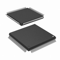
R5F2L3AAANFP#U1 Renesas Electronics America, R5F2L3AAANFP#U1 Datasheet - Page 235

R5F2L3AAANFP#U1
Manufacturer Part Number
R5F2L3AAANFP#U1
Description
MCU FLASH 96+4KB 100LQFP
Manufacturer
Renesas Electronics America
Series
R8C/Lx/3AAr
Datasheet
1.R5F2L387ANFPU1.pdf
(864 pages)
Specifications of R5F2L3AAANFP#U1
Core Processor
R8C
Core Size
16/32-Bit
Speed
20MHz
Connectivity
I²C, LIN, SIO, SSU, UART/USART
Peripherals
LCD, POR, PWM, Voltage Detect, WDT
Number Of I /o
88
Program Memory Size
96KB (96K x 8)
Program Memory Type
FLASH
Ram Size
10K x 8
Voltage - Supply (vcc/vdd)
1.8 V ~ 5.5 V
Data Converters
A/D 20x10b; D/A 2x8b
Oscillator Type
Internal
Operating Temperature
-20°C ~ 85°C
Package / Case
100-LQFP
Lead Free Status / RoHS Status
Lead free / RoHS Compliant
Eeprom Size
-
Available stocks
Company
Part Number
Manufacturer
Quantity
Price
- Current page: 235 of 864
- Download datasheet (16Mb)
R8C/L35A Group, R8C/L36A Group, R8C/L38A Group, R8C/L3AA Group,
R8C/L35B Group, R8C/L36B Group, R8C/L38B Group, R8C/L3AB Group
REJ09B0441-0100 Rev.1.00
Page 198 of 802
15. DTC
The DTC (data transfer controller) is a function that transfers data between the SFR and on-chip memory without using
the CPU. This chip incorporates one DTC channel. The DTC is activated by a peripheral function interrupt to perform
data transfers. The DTC and CPU use the same bus, and the DTC takes priority over the CPU in using the bus.
To control DTC data transfers, control data comprised of a transfer source address, a transfer destination address, and
operating modes are allocated in the DTC control data area. Each time the DTC is activated, the DTC reads control
data to perform data transfers.
15.1
Table 15.1
i = 0 to 6, j = 0 to 23
Activation sources
Allocatable control data
Address space which can be transferred
Maximum number of transfer
times
Maximum size of block to be
transferred
Unit of transfers
Transfer mode
Address control
Priority of activation sources
Interrupt request
Transfer start
Transfer stop
Table 15.1 lists the DTC Specifications and Figure 15.1 shows DTC Block Diagram.
Overview
DTC Specifications
Item
Oct 30, 2009
Normal mode
Repeat mode
Normal mode
Repeat mode
Normal mode
Repeat mode
Normal mode
Repeat mode
Normal mode
Repeat mode
Normal mode
Repeat mode
38 sources
24 sets
64 Kbytes (00000h to 0FFFFh)
256 times
255 times
256 bytes
255 bytes
Byte
Transfers end on completion of the transfer causing the DTCCTj
register value to change from 1 to 0.
On completion of the transfer causing the DTCCTj register value to
change from 1 to 0, the repeat area address is initialized and the
DTRLDj register value is reloaded to the DTCCTj register to continue
transfers.
Fixed or incremented
Addresses of the area not selected as the repeat area are fixed or
incremented.
See Table 15.5 DTC Activation Sources and DTC Vector
Addresses .
When the data transfer causing the DTCCTj register value to change
from 1 to 0 is performed, the activation source interrupt request is
generated for the CPU, and interrupt handling is performed on
completion of the data transfer.
When the data transfer causing the DTCCTj register value to change
from 1 to 0 is performed while the RPTINT bit in the DTCCRj register
is 1 (interrupt generation enabled), the activation source interrupt
request is generated for the CPU, and interrupt handling is performed
on completion of the transfer.
When bits DTCENi0 to DTCENi7 in the DTCENi registers are 1
(activation enabled), data transfer is started each time the
corresponding DTC activation sources are generated.
• When bits DTCENi0 to DTCENi7 are set to 0 (activation disabled).
• When the data transfer causing the DTCCTj register value to
• When bits DTCENi0 to DTCENi7 are set to 0 (activation disabled).
• When the data transfer causing the DTCCTj register value to
change from 1 to 0 is completed.
change from 1 to 0 is completed while the RPTINT bit is 1 (interrupt
generation enabled).
Specification
15. DTC
Related parts for R5F2L3AAANFP#U1
Image
Part Number
Description
Manufacturer
Datasheet
Request
R

Part Number:
Description:
KIT STARTER FOR M16C/29
Manufacturer:
Renesas Electronics America
Datasheet:

Part Number:
Description:
KIT STARTER FOR R8C/2D
Manufacturer:
Renesas Electronics America
Datasheet:

Part Number:
Description:
R0K33062P STARTER KIT
Manufacturer:
Renesas Electronics America
Datasheet:

Part Number:
Description:
KIT STARTER FOR R8C/23 E8A
Manufacturer:
Renesas Electronics America
Datasheet:

Part Number:
Description:
KIT STARTER FOR R8C/25
Manufacturer:
Renesas Electronics America
Datasheet:

Part Number:
Description:
KIT STARTER H8S2456 SHARPE DSPLY
Manufacturer:
Renesas Electronics America
Datasheet:

Part Number:
Description:
KIT STARTER FOR R8C38C
Manufacturer:
Renesas Electronics America
Datasheet:

Part Number:
Description:
KIT STARTER FOR R8C35C
Manufacturer:
Renesas Electronics America
Datasheet:

Part Number:
Description:
KIT STARTER FOR R8CL3AC+LCD APPS
Manufacturer:
Renesas Electronics America
Datasheet:

Part Number:
Description:
KIT STARTER FOR RX610
Manufacturer:
Renesas Electronics America
Datasheet:

Part Number:
Description:
KIT STARTER FOR R32C/118
Manufacturer:
Renesas Electronics America
Datasheet:

Part Number:
Description:
KIT DEV RSK-R8C/26-29
Manufacturer:
Renesas Electronics America
Datasheet:

Part Number:
Description:
KIT STARTER FOR SH7124
Manufacturer:
Renesas Electronics America
Datasheet:

Part Number:
Description:
KIT STARTER FOR H8SX/1622
Manufacturer:
Renesas Electronics America
Datasheet:

Part Number:
Description:
KIT DEV FOR SH7203
Manufacturer:
Renesas Electronics America
Datasheet:


