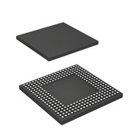
HD6417760BL200AV Renesas Electronics America, HD6417760BL200AV Datasheet - Page 1035

HD6417760BL200AV
Manufacturer Part Number
HD6417760BL200AV
Description
SH4 7760, 17 X17 256BGA, LCDC, U
Manufacturer
Renesas Electronics America
Series
SuperH® SH7750r
Datasheet
1.D6417760BP200ADV.pdf
(1418 pages)
Specifications of HD6417760BL200AV
Core Processor
SH-4
Core Size
32-Bit
Speed
200MHz
Connectivity
Audio Codec, CAN, EBI/EMI, FIFO, I²C, MFI, MMC, SCI, Serial Sound, SIM, SPI, USB
Peripherals
DMA, LCD, POR, WDT
Number Of I /o
69
Program Memory Type
ROMless
Ram Size
48K x 8
Voltage - Supply (vcc/vdd)
1.4 V ~ 1.6 V
Data Converters
A/D 4x10b
Oscillator Type
Internal
Operating Temperature
-40°C ~ 85°C
Package / Case
256-BGA
Lead Free Status / RoHS Status
Lead free / RoHS Compliant
Eeprom Size
-
Program Memory Size
-
Available stocks
Company
Part Number
Manufacturer
Quantity
Price
Company:
Part Number:
HD6417760BL200AV
Manufacturer:
Renesas Electronics America
Quantity:
10 000
Part Number:
HD6417760BL200AV
Manufacturer:
RENENAS
Quantity:
20 000
- Current page: 1035 of 1418
- Download datasheet (9Mb)
Some states of the multimedia card cause command sequence on the multimedia card side to stop.
Table 26.6 shows the card states in which a command sequence is halted. In this case, the
command sequence should also be aborted by setting the CMDOFF bit to 1 on the MMCIF side.
Table 26.6 Card States in which Command Sequence is Halted
In write data transmission, the contents of the command response and data response should be
analyzed, and then transmission should be triggered. In addition, the transfer clock (MCCLK)
output should be temporarily halted by FIFO full/empty, and it should be resumed when the
preparation has been completed.
Bit
4
3 to 0
Card Operating Mode
MMC mode
Bit
Name
DATAEN
—
Command response
Data status
Initial
Value
0
All 0
R/W
R/W
R
Error Status
When the error detection bit in the card status (32 bits)
in the command response data transmitted by the card
is set.
When the CRCERI bit is set due to an error in the CRC
status to be transmitted from the card is set while block
data is transmitted to the card.
Description
Data Enable
Starts write data transmission by a command with
write data. This bit is cleared automatically when 1 is
written. Resumes transfer clock output and write data
transmission when the transfer clock has been halted
by FIFO empty or termination of one block writing in
multiblock write.
Write enabled period: (1) after receiving a response to
a command with write data, (2) while transfer clock is
halted by FIFO empty, (3) when one block writing in
multiblock write is terminated
Write of 0: Operation is not affected.
Write of 1: Starts or resumes transfer clock output
Reserved
These bits are always read as 0. The write value
should always be 0.
and write data transmission.
Rev. 2.00 Feb. 12, 2010 Page 951 of 1330
REJ09B0554-0200
Related parts for HD6417760BL200AV
Image
Part Number
Description
Manufacturer
Datasheet
Request
R

Part Number:
Description:
KIT STARTER FOR M16C/29
Manufacturer:
Renesas Electronics America
Datasheet:

Part Number:
Description:
KIT STARTER FOR R8C/2D
Manufacturer:
Renesas Electronics America
Datasheet:

Part Number:
Description:
R0K33062P STARTER KIT
Manufacturer:
Renesas Electronics America
Datasheet:

Part Number:
Description:
KIT STARTER FOR R8C/23 E8A
Manufacturer:
Renesas Electronics America
Datasheet:

Part Number:
Description:
KIT STARTER FOR R8C/25
Manufacturer:
Renesas Electronics America
Datasheet:

Part Number:
Description:
KIT STARTER H8S2456 SHARPE DSPLY
Manufacturer:
Renesas Electronics America
Datasheet:

Part Number:
Description:
KIT STARTER FOR R8C38C
Manufacturer:
Renesas Electronics America
Datasheet:

Part Number:
Description:
KIT STARTER FOR R8C35C
Manufacturer:
Renesas Electronics America
Datasheet:

Part Number:
Description:
KIT STARTER FOR R8CL3AC+LCD APPS
Manufacturer:
Renesas Electronics America
Datasheet:

Part Number:
Description:
KIT STARTER FOR RX610
Manufacturer:
Renesas Electronics America
Datasheet:

Part Number:
Description:
KIT STARTER FOR R32C/118
Manufacturer:
Renesas Electronics America
Datasheet:

Part Number:
Description:
KIT DEV RSK-R8C/26-29
Manufacturer:
Renesas Electronics America
Datasheet:

Part Number:
Description:
KIT STARTER FOR SH7124
Manufacturer:
Renesas Electronics America
Datasheet:

Part Number:
Description:
KIT STARTER FOR H8SX/1622
Manufacturer:
Renesas Electronics America
Datasheet:

Part Number:
Description:
KIT DEV FOR SH7203
Manufacturer:
Renesas Electronics America
Datasheet:


