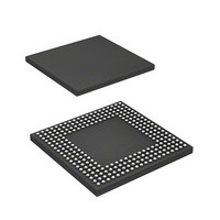
HD6417760BL200AV Renesas Electronics America, HD6417760BL200AV Datasheet - Page 1171

HD6417760BL200AV
Manufacturer Part Number
HD6417760BL200AV
Description
SH4 7760, 17 X17 256BGA, LCDC, U
Manufacturer
Renesas Electronics America
Series
SuperH® SH7750r
Datasheet
1.D6417760BP200ADV.pdf
(1418 pages)
Specifications of HD6417760BL200AV
Core Processor
SH-4
Core Size
32-Bit
Speed
200MHz
Connectivity
Audio Codec, CAN, EBI/EMI, FIFO, I²C, MFI, MMC, SCI, Serial Sound, SIM, SPI, USB
Peripherals
DMA, LCD, POR, WDT
Number Of I /o
69
Program Memory Type
ROMless
Ram Size
48K x 8
Voltage - Supply (vcc/vdd)
1.4 V ~ 1.6 V
Data Converters
A/D 4x10b
Oscillator Type
Internal
Operating Temperature
-40°C ~ 85°C
Package / Case
256-BGA
Lead Free Status / RoHS Status
Lead free / RoHS Compliant
Eeprom Size
-
Program Memory Size
-
Available stocks
Company
Part Number
Manufacturer
Quantity
Price
Company:
Part Number:
HD6417760BL200AV
Manufacturer:
Renesas Electronics America
Quantity:
10 000
Part Number:
HD6417760BL200AV
Manufacturer:
RENENAS
Quantity:
20 000
- Current page: 1171 of 1418
- Download datasheet (9Mb)
30.3.17 LCDC Power Management Mode Register (LDPMMR)
LDPMMR controls the power supply circuit that provides power to the LCD module. The usage
of two types of power-supply control pins, VCPWC and VEPWC, and turning on or off the power
supply function are selected.
Initial value:
Bit
15
14
13
12
11
10
9
8
7
6
R/W:
Bit:
Bit Name
ONC3
ONC2
ONC1
ONC0
OFFD3
OFFD2
OFFD1
OFFD0
⎯
VCPE
ONC3 ONC2 ONC1 ONC0 OFFD3 OFFD2 OFFD1 OFFD0
R/W
15
0
R/W
14
0
R/W
13
0
Initial Value
0
0
0
0
0
0
0
0
0
0
R/W
12
0
R/W
11
0
R/W
R/W
R/W
R/W
R/W
R/W
R/W
R/W
R/W
R/W
R
R/W
10
0
R/W
9
0
Description
LCDC Power-On Sequence Period
Sets the period from VEPWC assertion to
LCD_DON assertion in the power-on sequence of
the LCD module in frame units.
Specify a value of (the period) −1.
This period is the (c) period in figures 30.4 to 30.7,
Power-Supply Control Sequence and States of the
LCD Module. For details on setting this register, see
table 30.5, Available Power-Supply Control-
Sequence Periods at Typical Frame Rates. (The
setting method is common for ONA, ONB, OFFD,
OFFE, and OFFF.)
LCDC Power-Off Sequence Period
Sets the period from LCD_DON negation to
VEPWC negation in the power-off sequence of the
LCD module in frame units.
Specify a value of (the period) −1.
This period is the (d) period in figures 30.4 to 30.7,
Power-Supply Control Sequence and States of the
LCD Module.
Reserved
This bit is always read as 0. The write value should
always be 0.
VCPWC Pin Enable
Sets whether or not to enable a power-supply
control sequence using the VCPWC pin.
0: Disabled: VCPWC pin output is masked and
1: Enabled: VCPWC pin output is asserted and
fixed low
negated according to the power-on or power-off
sequence
R/W
8
0
0
R
7
-
Rev. 2.00 Feb. 12, 2010 Page 1087 of 1330
VCPE
R/W
6
0
VEPE
R/W
5
0
DONE
R/W
4
1
3
0
R
-
REJ09B0554-0200
R
2
0
-
LPS1
R
1
0
LPS0
R
0
0
Related parts for HD6417760BL200AV
Image
Part Number
Description
Manufacturer
Datasheet
Request
R

Part Number:
Description:
KIT STARTER FOR M16C/29
Manufacturer:
Renesas Electronics America
Datasheet:

Part Number:
Description:
KIT STARTER FOR R8C/2D
Manufacturer:
Renesas Electronics America
Datasheet:

Part Number:
Description:
R0K33062P STARTER KIT
Manufacturer:
Renesas Electronics America
Datasheet:

Part Number:
Description:
KIT STARTER FOR R8C/23 E8A
Manufacturer:
Renesas Electronics America
Datasheet:

Part Number:
Description:
KIT STARTER FOR R8C/25
Manufacturer:
Renesas Electronics America
Datasheet:

Part Number:
Description:
KIT STARTER H8S2456 SHARPE DSPLY
Manufacturer:
Renesas Electronics America
Datasheet:

Part Number:
Description:
KIT STARTER FOR R8C38C
Manufacturer:
Renesas Electronics America
Datasheet:

Part Number:
Description:
KIT STARTER FOR R8C35C
Manufacturer:
Renesas Electronics America
Datasheet:

Part Number:
Description:
KIT STARTER FOR R8CL3AC+LCD APPS
Manufacturer:
Renesas Electronics America
Datasheet:

Part Number:
Description:
KIT STARTER FOR RX610
Manufacturer:
Renesas Electronics America
Datasheet:

Part Number:
Description:
KIT STARTER FOR R32C/118
Manufacturer:
Renesas Electronics America
Datasheet:

Part Number:
Description:
KIT DEV RSK-R8C/26-29
Manufacturer:
Renesas Electronics America
Datasheet:

Part Number:
Description:
KIT STARTER FOR SH7124
Manufacturer:
Renesas Electronics America
Datasheet:

Part Number:
Description:
KIT STARTER FOR H8SX/1622
Manufacturer:
Renesas Electronics America
Datasheet:

Part Number:
Description:
KIT DEV FOR SH7203
Manufacturer:
Renesas Electronics America
Datasheet:


