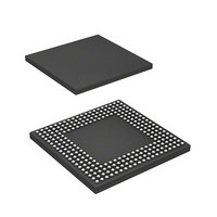
HD6417760BL200AV Renesas Electronics America, HD6417760BL200AV Datasheet - Page 1140

HD6417760BL200AV
Manufacturer Part Number
HD6417760BL200AV
Description
SH4 7760, 17 X17 256BGA, LCDC, U
Manufacturer
Renesas Electronics America
Series
SuperH® SH7750r
Datasheet
1.D6417760BP200ADV.pdf
(1418 pages)
Specifications of HD6417760BL200AV
Core Processor
SH-4
Core Size
32-Bit
Speed
200MHz
Connectivity
Audio Codec, CAN, EBI/EMI, FIFO, I²C, MFI, MMC, SCI, Serial Sound, SIM, SPI, USB
Peripherals
DMA, LCD, POR, WDT
Number Of I /o
69
Program Memory Type
ROMless
Ram Size
48K x 8
Voltage - Supply (vcc/vdd)
1.4 V ~ 1.6 V
Data Converters
A/D 4x10b
Oscillator Type
Internal
Operating Temperature
-40°C ~ 85°C
Package / Case
256-BGA
Lead Free Status / RoHS Status
Lead free / RoHS Compliant
Eeprom Size
-
Program Memory Size
-
Available stocks
Company
Part Number
Manufacturer
Quantity
Price
Company:
Part Number:
HD6417760BL200AV
Manufacturer:
Renesas Electronics America
Quantity:
10 000
Part Number:
HD6417760BL200AV
Manufacturer:
RENENAS
Quantity:
20 000
- Current page: 1140 of 1418
- Download datasheet (9Mb)
29.5
The A/D converter generates an interrupt (ADI) at the end of A/D conversion.
The ADI interrupt request is enabled/disabled by specifying the ADIE bit in ADCSR. Either
interrupt generation or DMAC activation when A/D conversion ends can be selected by the
DMASL bit.
Since data for only one channel can be DMA transferred for each interrupt, data for all specified
channels can not be DMA transferred when more than one channel is specified in multi or scan
mode.
29.6
The A/D converter compares an input for an analog channel to its analog reference voltage and
converts it into 10-bit digital data. The absolute accuracy of this A/D conversion is the deviation
between the input analog value and the output digital value. It includes the following errors:
1. Offset error (figure 29.7 (1))
2. Full-scale error (figure 29.7 (2))
3. Quantization error (figure 29.7 (3))
4. Nonlinearity error (figure 29.7 (4))
Rev. 2.00 Feb. 12, 2010 Page 1056 of 1330
REJ09B0554-0200
Deviation between analog input voltage and ideal A/D conversion characteristics when the
digital output value changes from the minimum (zero voltage) B'0000000000 (B'000 in figure
29.7) to B'0000000001 (B'001 in figure 29.7)
Deviation between analog input voltage and ideal A/D conversion characteristics when the
digital output value changes from the B'1111111110 (B'110 in figure 29.7) to the maximum
B'1111111111 (B'111 in figure 29.7).
Intrinsic error of the A/D converter and is expressed as 1/2 LSB.
Deviation between analog input voltage and ideal A/D conversion characteristics between zero
voltage and full-scale voltage. Note that it does not include offset, full-scale, and quantization
errors.
Definitions of A/D Conversion Accuracy
Interrupts
Related parts for HD6417760BL200AV
Image
Part Number
Description
Manufacturer
Datasheet
Request
R

Part Number:
Description:
KIT STARTER FOR M16C/29
Manufacturer:
Renesas Electronics America
Datasheet:

Part Number:
Description:
KIT STARTER FOR R8C/2D
Manufacturer:
Renesas Electronics America
Datasheet:

Part Number:
Description:
R0K33062P STARTER KIT
Manufacturer:
Renesas Electronics America
Datasheet:

Part Number:
Description:
KIT STARTER FOR R8C/23 E8A
Manufacturer:
Renesas Electronics America
Datasheet:

Part Number:
Description:
KIT STARTER FOR R8C/25
Manufacturer:
Renesas Electronics America
Datasheet:

Part Number:
Description:
KIT STARTER H8S2456 SHARPE DSPLY
Manufacturer:
Renesas Electronics America
Datasheet:

Part Number:
Description:
KIT STARTER FOR R8C38C
Manufacturer:
Renesas Electronics America
Datasheet:

Part Number:
Description:
KIT STARTER FOR R8C35C
Manufacturer:
Renesas Electronics America
Datasheet:

Part Number:
Description:
KIT STARTER FOR R8CL3AC+LCD APPS
Manufacturer:
Renesas Electronics America
Datasheet:

Part Number:
Description:
KIT STARTER FOR RX610
Manufacturer:
Renesas Electronics America
Datasheet:

Part Number:
Description:
KIT STARTER FOR R32C/118
Manufacturer:
Renesas Electronics America
Datasheet:

Part Number:
Description:
KIT DEV RSK-R8C/26-29
Manufacturer:
Renesas Electronics America
Datasheet:

Part Number:
Description:
KIT STARTER FOR SH7124
Manufacturer:
Renesas Electronics America
Datasheet:

Part Number:
Description:
KIT STARTER FOR H8SX/1622
Manufacturer:
Renesas Electronics America
Datasheet:

Part Number:
Description:
KIT DEV FOR SH7203
Manufacturer:
Renesas Electronics America
Datasheet:


