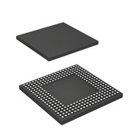
HD6417760BL200AV Renesas Electronics America, HD6417760BL200AV Datasheet - Page 345

HD6417760BL200AV
Manufacturer Part Number
HD6417760BL200AV
Description
SH4 7760, 17 X17 256BGA, LCDC, U
Manufacturer
Renesas Electronics America
Series
SuperH® SH7750r
Datasheet
1.D6417760BP200ADV.pdf
(1418 pages)
Specifications of HD6417760BL200AV
Core Processor
SH-4
Core Size
32-Bit
Speed
200MHz
Connectivity
Audio Codec, CAN, EBI/EMI, FIFO, I²C, MFI, MMC, SCI, Serial Sound, SIM, SPI, USB
Peripherals
DMA, LCD, POR, WDT
Number Of I /o
69
Program Memory Type
ROMless
Ram Size
48K x 8
Voltage - Supply (vcc/vdd)
1.4 V ~ 1.6 V
Data Converters
A/D 4x10b
Oscillator Type
Internal
Operating Temperature
-40°C ~ 85°C
Package / Case
256-BGA
Lead Free Status / RoHS Status
Lead free / RoHS Compliant
Eeprom Size
-
Program Memory Size
-
Available stocks
Company
Part Number
Manufacturer
Quantity
Price
Company:
Part Number:
HD6417760BL200AV
Manufacturer:
Renesas Electronics America
Quantity:
10 000
Part Number:
HD6417760BL200AV
Manufacturer:
RENENAS
Quantity:
20 000
- Current page: 345 of 1418
- Download datasheet (9Mb)
Bit
26
25
24
23, 22
21
20
Bit
Name
DPUP
⎯
OPUP
⎯
A1MBC
A4MBC
Initial
Value
0
0
0
All 0
0
0
R/W
R/W
R
R/W
R
R/W
R/W
Description
Data Pin Pull-Up Resistor Control
Specifies the pull-up resistor status of the data pins (D31
to D0). It is initialized by a power-on reset. The pins are
not pulled up when access is performed or when the bus
is released, even if the pull-up resistor is on.
0: Cycle is provided for turning on the pull-up resistor for
1: Pull-up resistor is off for data pins (D31 to D0).
Note: *It is recommended that a pull-up resistor be
Reserved
This bit is always read as 0. The write value should
always be 0.
Control Output Pin Pull-Up Resistor Control
Specifies the pull-up resistor status (A[25:0], BS, CSn,
RD, WEn, RD/WR, RAS, CE2A, CE2B) when the control
output pins are high-impedance. This bit is initialized by a
power-on reset.
0: Pull-up resistor is on for control output pins (A[25:0],
1: Pull-up resistor is off for control output pins (A[25:0],
Reserved
These bits are always read as 0. The write value should
always be 0.
Area 1 SRAM Byte Control Mode
MPX interface has priority when MPX interface is set.
This bit is initialized by a power-on reset.
0: Area 1 SRAM is set to normal mode
1: Area 1 SRAM is set to byte control mode
Area 4 SRAM Byte Control Mode
MPX interface has priority when MPX interface is set.
This bit is initialized by a power-on reset.
0: Area 4 SRAM is set to normal mode
1: Area 4 SRAM is set to byte control mode
data pins (D31 to D0) before and after memory
access.*
BS, CSn, RD, WEn, RD/WR, RAS, CE2A, CE2B)
BS, CSn, RD, WEn, RD/WR, RAS, CE2A, CE2B)
externally attached for the data pins if it is
required.
Rev. 2.00 Feb. 12, 2010 Page 261 of 1330
REJ09B0554-0200
Related parts for HD6417760BL200AV
Image
Part Number
Description
Manufacturer
Datasheet
Request
R

Part Number:
Description:
KIT STARTER FOR M16C/29
Manufacturer:
Renesas Electronics America
Datasheet:

Part Number:
Description:
KIT STARTER FOR R8C/2D
Manufacturer:
Renesas Electronics America
Datasheet:

Part Number:
Description:
R0K33062P STARTER KIT
Manufacturer:
Renesas Electronics America
Datasheet:

Part Number:
Description:
KIT STARTER FOR R8C/23 E8A
Manufacturer:
Renesas Electronics America
Datasheet:

Part Number:
Description:
KIT STARTER FOR R8C/25
Manufacturer:
Renesas Electronics America
Datasheet:

Part Number:
Description:
KIT STARTER H8S2456 SHARPE DSPLY
Manufacturer:
Renesas Electronics America
Datasheet:

Part Number:
Description:
KIT STARTER FOR R8C38C
Manufacturer:
Renesas Electronics America
Datasheet:

Part Number:
Description:
KIT STARTER FOR R8C35C
Manufacturer:
Renesas Electronics America
Datasheet:

Part Number:
Description:
KIT STARTER FOR R8CL3AC+LCD APPS
Manufacturer:
Renesas Electronics America
Datasheet:

Part Number:
Description:
KIT STARTER FOR RX610
Manufacturer:
Renesas Electronics America
Datasheet:

Part Number:
Description:
KIT STARTER FOR R32C/118
Manufacturer:
Renesas Electronics America
Datasheet:

Part Number:
Description:
KIT DEV RSK-R8C/26-29
Manufacturer:
Renesas Electronics America
Datasheet:

Part Number:
Description:
KIT STARTER FOR SH7124
Manufacturer:
Renesas Electronics America
Datasheet:

Part Number:
Description:
KIT STARTER FOR H8SX/1622
Manufacturer:
Renesas Electronics America
Datasheet:

Part Number:
Description:
KIT DEV FOR SH7203
Manufacturer:
Renesas Electronics America
Datasheet:


