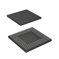
HD6417760BL200AV Renesas Electronics America, HD6417760BL200AV Datasheet - Page 777

HD6417760BL200AV
Manufacturer Part Number
HD6417760BL200AV
Description
SH4 7760, 17 X17 256BGA, LCDC, U
Manufacturer
Renesas Electronics America
Series
SuperH® SH7750r
Datasheet
1.D6417760BP200ADV.pdf
(1418 pages)
Specifications of HD6417760BL200AV
Core Processor
SH-4
Core Size
32-Bit
Speed
200MHz
Connectivity
Audio Codec, CAN, EBI/EMI, FIFO, I²C, MFI, MMC, SCI, Serial Sound, SIM, SPI, USB
Peripherals
DMA, LCD, POR, WDT
Number Of I /o
69
Program Memory Type
ROMless
Ram Size
48K x 8
Voltage - Supply (vcc/vdd)
1.4 V ~ 1.6 V
Data Converters
A/D 4x10b
Oscillator Type
Internal
Operating Temperature
-40°C ~ 85°C
Package / Case
256-BGA
Lead Free Status / RoHS Status
Lead free / RoHS Compliant
Eeprom Size
-
Program Memory Size
-
Available stocks
Company
Part Number
Manufacturer
Quantity
Price
Company:
Part Number:
HD6417760BL200AV
Manufacturer:
Renesas Electronics America
Quantity:
10 000
Part Number:
HD6417760BL200AV
Manufacturer:
RENENAS
Quantity:
20 000
- Current page: 777 of 1418
- Download datasheet (9Mb)
Figure 19.8 shows the data transmit/receive combination format
In the data transmit/receive combination format, data is transmitted after an address is transmitted
with the first two bytes. Then, retransmit condition (Sr) is transmitted instead of stop condition
(P). After Sr is transmitted, the procedure is the same as that in the data receive format.
19.4.8
This section describes the transmit procedure and operations in master transmit mode. Figures
19.9 to 19.11 are the timing charts in master transmit mode. Setting the MDBS bit to 1 in the
master control register has the I
1. For initial setting, set clock control bits in the clock control register and interrupt generation
2. Monitor the FSDA bit in the master control register. Confirm that the bit is low, which means
3. After the signals for indicating the transmit start condition, the slave address, and the data
4. Interrupt indicated by the SAR is generated in the timing of (3) in figure 19.9. If the IRQ
bits in the master interrupt enable register, according to the slave address, transmit data, and
the transmit speed. Since the slave mode is also required even when only the master mode is
used, set the device address to the slave address register.
Do not modify either the master control register MDBS bit or the slave control register SDBS
bit during operation. Incorrect operation may occur if these bits are changed during operation.
that the other I
in the master control register to 1 to start master transmission.
transfer direction are transmitted, an interrupt indicated by the MDE bit and the MAT bit in the
master status register is generated in the timing of (1) in figure 19.9. At this time, clear the
ESG bit to 0. The master device holds SCL low to suspend data transmission until the MDE bit
is cleared to 0.
processing of the slave device is delayed, the slave device extends the SCL period to suspend
data transmission (in the timing of (7) in figure 19.9). The slave device drives SDA low at the
ninth clock and returns ACK.
Master Transmit Operation (Single Buffer Mode)
S
Figure 19.8 10-Bit Address Transmit/Receive Combination Format
1st 7bits of 1st byte
SLAVE ADDRESS
1 1 1 1 0 X X
2
C device is not using the bus. After confirmation, set the MIE bit and ESG bit
0 (Write)
2
R/W A1
C module enter single buffer mode.
Sr
1st 7 bits of 1st byte
SLAVE ADDRESS
SLAVE ADDRESS
1 1 1 1 0 X X
SLAVE ADDRESS
2nd byte
1 (Read)
R/W
A2
A3
Rev. 2.00 Feb. 12, 2010 Page 693 of 1330
DATA
DATA
Data transferred
Data transferred
A
A
DATA
Section 19 I
DATA
A/A
REJ09B0554-0200
A
2
C Bus Interface
P
Related parts for HD6417760BL200AV
Image
Part Number
Description
Manufacturer
Datasheet
Request
R

Part Number:
Description:
KIT STARTER FOR M16C/29
Manufacturer:
Renesas Electronics America
Datasheet:

Part Number:
Description:
KIT STARTER FOR R8C/2D
Manufacturer:
Renesas Electronics America
Datasheet:

Part Number:
Description:
R0K33062P STARTER KIT
Manufacturer:
Renesas Electronics America
Datasheet:

Part Number:
Description:
KIT STARTER FOR R8C/23 E8A
Manufacturer:
Renesas Electronics America
Datasheet:

Part Number:
Description:
KIT STARTER FOR R8C/25
Manufacturer:
Renesas Electronics America
Datasheet:

Part Number:
Description:
KIT STARTER H8S2456 SHARPE DSPLY
Manufacturer:
Renesas Electronics America
Datasheet:

Part Number:
Description:
KIT STARTER FOR R8C38C
Manufacturer:
Renesas Electronics America
Datasheet:

Part Number:
Description:
KIT STARTER FOR R8C35C
Manufacturer:
Renesas Electronics America
Datasheet:

Part Number:
Description:
KIT STARTER FOR R8CL3AC+LCD APPS
Manufacturer:
Renesas Electronics America
Datasheet:

Part Number:
Description:
KIT STARTER FOR RX610
Manufacturer:
Renesas Electronics America
Datasheet:

Part Number:
Description:
KIT STARTER FOR R32C/118
Manufacturer:
Renesas Electronics America
Datasheet:

Part Number:
Description:
KIT DEV RSK-R8C/26-29
Manufacturer:
Renesas Electronics America
Datasheet:

Part Number:
Description:
KIT STARTER FOR SH7124
Manufacturer:
Renesas Electronics America
Datasheet:

Part Number:
Description:
KIT STARTER FOR H8SX/1622
Manufacturer:
Renesas Electronics America
Datasheet:

Part Number:
Description:
KIT DEV FOR SH7203
Manufacturer:
Renesas Electronics America
Datasheet:


