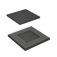
HD6417760BL200AV Renesas Electronics America, HD6417760BL200AV Datasheet - Page 130

HD6417760BL200AV
Manufacturer Part Number
HD6417760BL200AV
Description
SH4 7760, 17 X17 256BGA, LCDC, U
Manufacturer
Renesas Electronics America
Series
SuperH® SH7750r
Datasheet
1.D6417760BP200ADV.pdf
(1418 pages)
Specifications of HD6417760BL200AV
Core Processor
SH-4
Core Size
32-Bit
Speed
200MHz
Connectivity
Audio Codec, CAN, EBI/EMI, FIFO, I²C, MFI, MMC, SCI, Serial Sound, SIM, SPI, USB
Peripherals
DMA, LCD, POR, WDT
Number Of I /o
69
Program Memory Type
ROMless
Ram Size
48K x 8
Voltage - Supply (vcc/vdd)
1.4 V ~ 1.6 V
Data Converters
A/D 4x10b
Oscillator Type
Internal
Operating Temperature
-40°C ~ 85°C
Package / Case
256-BGA
Lead Free Status / RoHS Status
Lead free / RoHS Compliant
Eeprom Size
-
Program Memory Size
-
Available stocks
Company
Part Number
Manufacturer
Quantity
Price
Company:
Part Number:
HD6417760BL200AV
Manufacturer:
Renesas Electronics America
Quantity:
10 000
Part Number:
HD6417760BL200AV
Manufacturer:
RENENAS
Quantity:
20 000
- Current page: 130 of 1418
- Download datasheet (9Mb)
Saved General Register 15 (SGR): The contents of R15 are saved to SGR in the event of an
exception or interrupt.
Debug Base Register (DBR): When the user break debugging function is enabled (BRCR.UBDE
= 1), DBR is referenced as the branch destination address of the user break handler instead of
VBR.
2.2.4
The system registers are 32 bits long. They consist of two multiply-and-accumulate registers
(MACH and MACL), the procedure register (PR), the program counter (PC), the floating-point
status/control register (FPSCR), and the floating-point communication register (FPUL). For details
on FPSCR and FPUL, see section 3, Floating-Point Unit (FPU).
Multiply-and-Accumulate Registers (MACH and MACL): MACH and MACL are used for the
added value in a MAC instruction, and to store the operation result of a MAC or MUL instruction.
Procedure Register (PR): The return address is stored in PR in a subroutine call using a BSR,
BSRF, or JSR instruction. PR is referenced by the subroutine return instruction (RTS).
Program Counter (PC): PC indicates the address of the instruction currently being executed.
2.2.5
See section 3, Floating-Point Unit (FPU).
2.3
For details on the control registers mapped to memory, see section 32, List of Registers. The
control registers are double-mapped to the following two memory areas. All registers have two
addresses.
H'1C00 0000 to H'1FFF FFFF
H'FC00 0000 to H'FFFF FFFF
These two areas are used as follows.
• H'1C00 0000 to H'1FFF FFFF
Rev. 2.00 Feb. 12, 2010 Page 46 of 1330
REJ09B0554-0200
This area must be accessed using the address translation function of the MMU.
Setting the page number of this area to the corresponding field of the TLB enables access to a
memory-mapped register.
The operation of an access to this area without using the address translation function of the
MMU is not guaranteed.
System Registers
FPU Registers
Memory-Mapped Registers
Related parts for HD6417760BL200AV
Image
Part Number
Description
Manufacturer
Datasheet
Request
R

Part Number:
Description:
KIT STARTER FOR M16C/29
Manufacturer:
Renesas Electronics America
Datasheet:

Part Number:
Description:
KIT STARTER FOR R8C/2D
Manufacturer:
Renesas Electronics America
Datasheet:

Part Number:
Description:
R0K33062P STARTER KIT
Manufacturer:
Renesas Electronics America
Datasheet:

Part Number:
Description:
KIT STARTER FOR R8C/23 E8A
Manufacturer:
Renesas Electronics America
Datasheet:

Part Number:
Description:
KIT STARTER FOR R8C/25
Manufacturer:
Renesas Electronics America
Datasheet:

Part Number:
Description:
KIT STARTER H8S2456 SHARPE DSPLY
Manufacturer:
Renesas Electronics America
Datasheet:

Part Number:
Description:
KIT STARTER FOR R8C38C
Manufacturer:
Renesas Electronics America
Datasheet:

Part Number:
Description:
KIT STARTER FOR R8C35C
Manufacturer:
Renesas Electronics America
Datasheet:

Part Number:
Description:
KIT STARTER FOR R8CL3AC+LCD APPS
Manufacturer:
Renesas Electronics America
Datasheet:

Part Number:
Description:
KIT STARTER FOR RX610
Manufacturer:
Renesas Electronics America
Datasheet:

Part Number:
Description:
KIT STARTER FOR R32C/118
Manufacturer:
Renesas Electronics America
Datasheet:

Part Number:
Description:
KIT DEV RSK-R8C/26-29
Manufacturer:
Renesas Electronics America
Datasheet:

Part Number:
Description:
KIT STARTER FOR SH7124
Manufacturer:
Renesas Electronics America
Datasheet:

Part Number:
Description:
KIT STARTER FOR H8SX/1622
Manufacturer:
Renesas Electronics America
Datasheet:

Part Number:
Description:
KIT DEV FOR SH7203
Manufacturer:
Renesas Electronics America
Datasheet:


