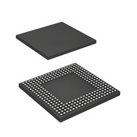
HD6417760BL200AV Renesas Electronics America, HD6417760BL200AV Datasheet - Page 459

HD6417760BL200AV
Manufacturer Part Number
HD6417760BL200AV
Description
SH4 7760, 17 X17 256BGA, LCDC, U
Manufacturer
Renesas Electronics America
Series
SuperH® SH7750r
Datasheet
1.D6417760BP200ADV.pdf
(1418 pages)
Specifications of HD6417760BL200AV
Core Processor
SH-4
Core Size
32-Bit
Speed
200MHz
Connectivity
Audio Codec, CAN, EBI/EMI, FIFO, I²C, MFI, MMC, SCI, Serial Sound, SIM, SPI, USB
Peripherals
DMA, LCD, POR, WDT
Number Of I /o
69
Program Memory Type
ROMless
Ram Size
48K x 8
Voltage - Supply (vcc/vdd)
1.4 V ~ 1.6 V
Data Converters
A/D 4x10b
Oscillator Type
Internal
Operating Temperature
-40°C ~ 85°C
Package / Case
256-BGA
Lead Free Status / RoHS Status
Lead free / RoHS Compliant
Eeprom Size
-
Program Memory Size
-
Available stocks
Company
Part Number
Manufacturer
Quantity
Price
Company:
Part Number:
HD6417760BL200AV
Manufacturer:
Renesas Electronics America
Quantity:
10 000
Part Number:
HD6417760BL200AV
Manufacturer:
RENENAS
Quantity:
20 000
- Current page: 459 of 1418
- Download datasheet (9Mb)
10.6.10 Bus Arbitration
This LSI provides a bus arbitration function that allows an off-chip device to control the bus in
response to a bus request.
In normal operation, this LSI controls the bus, and it releases the bus to transfer the right to access
the bus when an off-chip device issues a bus request. In the description below, an off-chip device
that issues bus requests is referred to as a slave.
This LSI has two internal bus masters: the CPU and DMAC. When synchronous DRAM is
connected and refresh control is performed, the refresh request serves as the third bus master. Bus
requests from off-chip devices are also added when this LSI is in master mode. If requests occur
simultaneously, the priority from highest to lowest is based on the following order: bus request
from an off-chip device, the refresh request, the DMAC, and the CPU.
To prevent malfunctions of connected devices when the right to access the bus is transferred from
master to slave, all bus control signals are negated before the bus is released. When the right of
access to the bus is received, bus control signals switch from the negated level to start driving the
CKIO
A25−A0
CSm
CSn
BS
RD/WR
RD
D31−D0
Read from Area m space
T1
access cycles specified for Area m
Wait cycle insertion between
Figure 10.60 Wait Cycles between Access Cycles
T2
Twait
Read from Area n space
T1
access cycles specified for Area n
T2
Wait cycle insertion between
Rev. 2.00 Feb. 12, 2010 Page 375 of 1330
Twait
Write to Area n space
T1
T2
REJ09B0554-0200
Related parts for HD6417760BL200AV
Image
Part Number
Description
Manufacturer
Datasheet
Request
R

Part Number:
Description:
KIT STARTER FOR M16C/29
Manufacturer:
Renesas Electronics America
Datasheet:

Part Number:
Description:
KIT STARTER FOR R8C/2D
Manufacturer:
Renesas Electronics America
Datasheet:

Part Number:
Description:
R0K33062P STARTER KIT
Manufacturer:
Renesas Electronics America
Datasheet:

Part Number:
Description:
KIT STARTER FOR R8C/23 E8A
Manufacturer:
Renesas Electronics America
Datasheet:

Part Number:
Description:
KIT STARTER FOR R8C/25
Manufacturer:
Renesas Electronics America
Datasheet:

Part Number:
Description:
KIT STARTER H8S2456 SHARPE DSPLY
Manufacturer:
Renesas Electronics America
Datasheet:

Part Number:
Description:
KIT STARTER FOR R8C38C
Manufacturer:
Renesas Electronics America
Datasheet:

Part Number:
Description:
KIT STARTER FOR R8C35C
Manufacturer:
Renesas Electronics America
Datasheet:

Part Number:
Description:
KIT STARTER FOR R8CL3AC+LCD APPS
Manufacturer:
Renesas Electronics America
Datasheet:

Part Number:
Description:
KIT STARTER FOR RX610
Manufacturer:
Renesas Electronics America
Datasheet:

Part Number:
Description:
KIT STARTER FOR R32C/118
Manufacturer:
Renesas Electronics America
Datasheet:

Part Number:
Description:
KIT DEV RSK-R8C/26-29
Manufacturer:
Renesas Electronics America
Datasheet:

Part Number:
Description:
KIT STARTER FOR SH7124
Manufacturer:
Renesas Electronics America
Datasheet:

Part Number:
Description:
KIT STARTER FOR H8SX/1622
Manufacturer:
Renesas Electronics America
Datasheet:

Part Number:
Description:
KIT DEV FOR SH7203
Manufacturer:
Renesas Electronics America
Datasheet:


