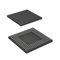
HD6417760BL200AV Renesas Electronics America, HD6417760BL200AV Datasheet - Page 825

HD6417760BL200AV
Manufacturer Part Number
HD6417760BL200AV
Description
SH4 7760, 17 X17 256BGA, LCDC, U
Manufacturer
Renesas Electronics America
Series
SuperH® SH7750r
Datasheet
1.D6417760BP200ADV.pdf
(1418 pages)
Specifications of HD6417760BL200AV
Core Processor
SH-4
Core Size
32-Bit
Speed
200MHz
Connectivity
Audio Codec, CAN, EBI/EMI, FIFO, I²C, MFI, MMC, SCI, Serial Sound, SIM, SPI, USB
Peripherals
DMA, LCD, POR, WDT
Number Of I /o
69
Program Memory Type
ROMless
Ram Size
48K x 8
Voltage - Supply (vcc/vdd)
1.4 V ~ 1.6 V
Data Converters
A/D 4x10b
Oscillator Type
Internal
Operating Temperature
-40°C ~ 85°C
Package / Case
256-BGA
Lead Free Status / RoHS Status
Lead free / RoHS Compliant
Eeprom Size
-
Program Memory Size
-
Available stocks
Company
Part Number
Manufacturer
Quantity
Price
Company:
Part Number:
HD6417760BL200AV
Manufacturer:
Renesas Electronics America
Quantity:
10 000
Part Number:
HD6417760BL200AV
Manufacturer:
RENENAS
Quantity:
20 000
- Current page: 825 of 1418
- Download datasheet (9Mb)
receiver case, the host CPU can skip forward storing null sample data until it is ready to store the
sample data that the SSI module is indicating that it will receive next to ensure consistency of the
number of received data, and so resynchronize with the audio data stream.
20.4.7
This function is used to control and select which clock is used for the serial bus interface.
If the serial clock direction is set to input (SCKD = 0), the SSI module is in clock slave mode, then
the bit clock that is used in the shift register is derived from the SSI_SCK pin.
If the serial clock direction is set to output (SCKD = 1), the SSI Module is in clock master mode,
and the shift register uses the bit clock derived from the HAC_BIT_CLK input pin or its clock
divided. This input clock is then divided by the ratio in the serial oversampling clock division ratio
(CKDV) bit in SSICR and used as the bit clock in the shift register.
In either case, the SSI_SCK pin output is the same as the bit clock.
20.5
20.5.1
If an overflow occurs during receive DMA operation, the module must be reactivated. If an
overflow occurs, recover the module according to the following procedure.
1. Ensure an overflow occurs through an overflow error interrupt or overflow error status flag
2. Terminate the DMA by writing 1 to the RDS bit in DMAACR. At this time, confirm the DMA
3.
4.
5.
6.
7. Reactivate the module by enabling the SSI module and DMA again.
(the OIRQ bit in SSISR).
is terminated by reading in the RDS bit (0 can be read).
Disable the DMA in the SSI module to halt its operation by writing 0 to the EN bit and
DMEN bit in SSICR.
Confirm the remaining number of the DMA by reading the DMAARXTCNT to reset the start
address of the DMA and number of transfers (MDAARXDAR/DMAARXTCR).
Clear the overflow status flag by writing 0 to the OIRQ bit.
Reactivate the DMAC by writing 1 to the RDE bit in DMAACR.
Restrictions when an Overflow Occurs during Receive DMA Operation
Serial Clock Control
Usage Note
Rev. 2.00 Feb. 12, 2010 Page 741 of 1330
REJ09B0554-0200
Related parts for HD6417760BL200AV
Image
Part Number
Description
Manufacturer
Datasheet
Request
R

Part Number:
Description:
KIT STARTER FOR M16C/29
Manufacturer:
Renesas Electronics America
Datasheet:

Part Number:
Description:
KIT STARTER FOR R8C/2D
Manufacturer:
Renesas Electronics America
Datasheet:

Part Number:
Description:
R0K33062P STARTER KIT
Manufacturer:
Renesas Electronics America
Datasheet:

Part Number:
Description:
KIT STARTER FOR R8C/23 E8A
Manufacturer:
Renesas Electronics America
Datasheet:

Part Number:
Description:
KIT STARTER FOR R8C/25
Manufacturer:
Renesas Electronics America
Datasheet:

Part Number:
Description:
KIT STARTER H8S2456 SHARPE DSPLY
Manufacturer:
Renesas Electronics America
Datasheet:

Part Number:
Description:
KIT STARTER FOR R8C38C
Manufacturer:
Renesas Electronics America
Datasheet:

Part Number:
Description:
KIT STARTER FOR R8C35C
Manufacturer:
Renesas Electronics America
Datasheet:

Part Number:
Description:
KIT STARTER FOR R8CL3AC+LCD APPS
Manufacturer:
Renesas Electronics America
Datasheet:

Part Number:
Description:
KIT STARTER FOR RX610
Manufacturer:
Renesas Electronics America
Datasheet:

Part Number:
Description:
KIT STARTER FOR R32C/118
Manufacturer:
Renesas Electronics America
Datasheet:

Part Number:
Description:
KIT DEV RSK-R8C/26-29
Manufacturer:
Renesas Electronics America
Datasheet:

Part Number:
Description:
KIT STARTER FOR SH7124
Manufacturer:
Renesas Electronics America
Datasheet:

Part Number:
Description:
KIT STARTER FOR H8SX/1622
Manufacturer:
Renesas Electronics America
Datasheet:

Part Number:
Description:
KIT DEV FOR SH7203
Manufacturer:
Renesas Electronics America
Datasheet:


