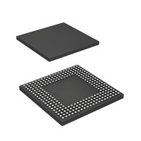
HD6417760BL200AV Renesas Electronics America, HD6417760BL200AV Datasheet - Page 948

HD6417760BL200AV
Manufacturer Part Number
HD6417760BL200AV
Description
SH4 7760, 17 X17 256BGA, LCDC, U
Manufacturer
Renesas Electronics America
Series
SuperH® SH7750r
Datasheet
1.D6417760BP200ADV.pdf
(1418 pages)
Specifications of HD6417760BL200AV
Core Processor
SH-4
Core Size
32-Bit
Speed
200MHz
Connectivity
Audio Codec, CAN, EBI/EMI, FIFO, I²C, MFI, MMC, SCI, Serial Sound, SIM, SPI, USB
Peripherals
DMA, LCD, POR, WDT
Number Of I /o
69
Program Memory Type
ROMless
Ram Size
48K x 8
Voltage - Supply (vcc/vdd)
1.4 V ~ 1.6 V
Data Converters
A/D 4x10b
Oscillator Type
Internal
Operating Temperature
-40°C ~ 85°C
Package / Case
256-BGA
Lead Free Status / RoHS Status
Lead free / RoHS Compliant
Eeprom Size
-
Program Memory Size
-
Available stocks
Company
Part Number
Manufacturer
Quantity
Price
Company:
Part Number:
HD6417760BL200AV
Manufacturer:
Renesas Electronics America
Quantity:
10 000
Part Number:
HD6417760BL200AV
Manufacturer:
RENENAS
Quantity:
20 000
- Current page: 948 of 1418
- Download datasheet (9Mb)
23.4.5
If any of the FBS, CLKP, IDIV or CLKC bit values are changed, then the HSPI software reset is
generated. The receive and transmit FIFO pointers can be initialized by the HSPI software reset.
The data transmission after the HSPI software reset should protect transmitting and receiving
protocol of HSPI, and please perform it from the first. A guarantee of operation is not offered
other than it.
23.4.6
SPCR also allows the user to define the shift timing for transmit data and polarity. The FBS bit in
SPCR allows selection between two different transfer formats. The MSB or LSB is valid on the
falling edge of HSPI_CS. The CLKP bit in SPCR allows for control of the polarity select block
which controls which edges of HSPI_CLK shift and sample data in the master and slave.
23.4.7
The master and slave can be considered linked together as a circular shift register synchronized
with HSPI_CLK. The transmit byte from the master is replaced with the receive byte from the
slave in eight HSPI_CLK cycles. Both the transmit and receive functions are double buffered to
allow for continuous reads and writes. When FIFO mode is enabled eight entry FIFOs are
available for both transmit and receive data.
Rev. 2.00 Feb. 12, 2010 Page 864 of 1330
REJ09B0554-0200
HSPI Software Reset
Clock Polarity and Transmit Control
Transmit and Receive Routines
HSPI_CLK (CLKP = 0)
HSPI_CLK (CLKP = 1)
Data transfer cycle
HSPI_RX
HSPI_CS
HSPI_TX
Figure 23.4 Timing Conditions when FBS = 1
*
MSB
MSB
1
2
6
6
3
5
5
4
4
4
5
3
3
6
2
2
7
1
1
LSB
8
LSB
Related parts for HD6417760BL200AV
Image
Part Number
Description
Manufacturer
Datasheet
Request
R

Part Number:
Description:
KIT STARTER FOR M16C/29
Manufacturer:
Renesas Electronics America
Datasheet:

Part Number:
Description:
KIT STARTER FOR R8C/2D
Manufacturer:
Renesas Electronics America
Datasheet:

Part Number:
Description:
R0K33062P STARTER KIT
Manufacturer:
Renesas Electronics America
Datasheet:

Part Number:
Description:
KIT STARTER FOR R8C/23 E8A
Manufacturer:
Renesas Electronics America
Datasheet:

Part Number:
Description:
KIT STARTER FOR R8C/25
Manufacturer:
Renesas Electronics America
Datasheet:

Part Number:
Description:
KIT STARTER H8S2456 SHARPE DSPLY
Manufacturer:
Renesas Electronics America
Datasheet:

Part Number:
Description:
KIT STARTER FOR R8C38C
Manufacturer:
Renesas Electronics America
Datasheet:

Part Number:
Description:
KIT STARTER FOR R8C35C
Manufacturer:
Renesas Electronics America
Datasheet:

Part Number:
Description:
KIT STARTER FOR R8CL3AC+LCD APPS
Manufacturer:
Renesas Electronics America
Datasheet:

Part Number:
Description:
KIT STARTER FOR RX610
Manufacturer:
Renesas Electronics America
Datasheet:

Part Number:
Description:
KIT STARTER FOR R32C/118
Manufacturer:
Renesas Electronics America
Datasheet:

Part Number:
Description:
KIT DEV RSK-R8C/26-29
Manufacturer:
Renesas Electronics America
Datasheet:

Part Number:
Description:
KIT STARTER FOR SH7124
Manufacturer:
Renesas Electronics America
Datasheet:

Part Number:
Description:
KIT STARTER FOR H8SX/1622
Manufacturer:
Renesas Electronics America
Datasheet:

Part Number:
Description:
KIT DEV FOR SH7203
Manufacturer:
Renesas Electronics America
Datasheet:


