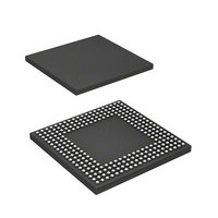
HD6417760BL200AV Renesas Electronics America, HD6417760BL200AV Datasheet - Page 1410

HD6417760BL200AV
Manufacturer Part Number
HD6417760BL200AV
Description
SH4 7760, 17 X17 256BGA, LCDC, U
Manufacturer
Renesas Electronics America
Series
SuperH® SH7750r
Datasheet
1.D6417760BP200ADV.pdf
(1418 pages)
Specifications of HD6417760BL200AV
Core Processor
SH-4
Core Size
32-Bit
Speed
200MHz
Connectivity
Audio Codec, CAN, EBI/EMI, FIFO, I²C, MFI, MMC, SCI, Serial Sound, SIM, SPI, USB
Peripherals
DMA, LCD, POR, WDT
Number Of I /o
69
Program Memory Type
ROMless
Ram Size
48K x 8
Voltage - Supply (vcc/vdd)
1.4 V ~ 1.6 V
Data Converters
A/D 4x10b
Oscillator Type
Internal
Operating Temperature
-40°C ~ 85°C
Package / Case
256-BGA
Lead Free Status / RoHS Status
Lead free / RoHS Compliant
Eeprom Size
-
Program Memory Size
-
Available stocks
Company
Part Number
Manufacturer
Quantity
Price
Company:
Part Number:
HD6417760BL200AV
Manufacturer:
Renesas Electronics America
Quantity:
10 000
Part Number:
HD6417760BL200AV
Manufacturer:
RENENAS
Quantity:
20 000
- Current page: 1410 of 1418
- Download datasheet (9Mb)
F.2
(1) Turn off the power supply of I/O and CPG to the same timing as the power supply VDDQ.
(2) There is no timing regulation of a signal line (RESET and MRESET).
(3) The input level to the pin must be lowered in compliance with the I/O, RTC, CPG power
(4) It recommends that turning off the I/O, CPG power supply voltage (VDDQ) after turning off
(5) In addition to the above (1), (2), (3), (4), and following (i), (ii), follow “F.3, The Ratings for
F.3
The LSI may be damaged when not satisfying the conditions of (1), (2), (3), and (4) below.
(1) VDDQ = VDD-CPG = AVCC–ADC
(2) VDD = VDD–PLL1 = VDD–PLL2 = VDD–PLL3
(3) –0.3V < VDD < VDDQ +0.3 V.
(4) VSS = VSSQ = VSS–PLL1=VSS–PLL2 = VSS–PLL3 = VSS–CPG = AVSS–ADC = GND
Rev. 2.00 Feb. 12, 2010 Page 1326 of 1330
REJ09B0554-0200
supply voltage.
the internal power supply voltage (VDD).
Power-on and Power-off”.
(i) In the case of this LSI simple substance, the power supply sequence of a power supply to
(ii) When this LSI is connected with other elements on the mounting board, please keep that
–0.3 V < VDD–PLL1 < VDDQ +0.3 V.
–0.3 V < VDD–PLL2 < VDDQ +0.3 V.
–0.3 V < VDD–PLL3 < VDDQ +0.3 V.
[0V].
VDDQ and VDD does not have time restrictions. Refer to figure F.1. In addition, it
recommends performing a power off at the shortest possible time.
–0.3 V < Vin < VDDQ +0.3 V.
Moreover, as shown in figure F.2, power down time (tpwd) until it goes down from an
operation voltage value {VDDQ (min), VDD (min)} to the following condition (B) is 150
ms (max).
If it is longer than that time, the LSI may be damaged.
In addition, it recommends performing a power off at the shortest possible time.
Condition (B): VDDQ < 1.0 V and VDD < 0.5 V
Power-off Procedure
The Ratings for Power-on and Power-off
Related parts for HD6417760BL200AV
Image
Part Number
Description
Manufacturer
Datasheet
Request
R

Part Number:
Description:
KIT STARTER FOR M16C/29
Manufacturer:
Renesas Electronics America
Datasheet:

Part Number:
Description:
KIT STARTER FOR R8C/2D
Manufacturer:
Renesas Electronics America
Datasheet:

Part Number:
Description:
R0K33062P STARTER KIT
Manufacturer:
Renesas Electronics America
Datasheet:

Part Number:
Description:
KIT STARTER FOR R8C/23 E8A
Manufacturer:
Renesas Electronics America
Datasheet:

Part Number:
Description:
KIT STARTER FOR R8C/25
Manufacturer:
Renesas Electronics America
Datasheet:

Part Number:
Description:
KIT STARTER H8S2456 SHARPE DSPLY
Manufacturer:
Renesas Electronics America
Datasheet:

Part Number:
Description:
KIT STARTER FOR R8C38C
Manufacturer:
Renesas Electronics America
Datasheet:

Part Number:
Description:
KIT STARTER FOR R8C35C
Manufacturer:
Renesas Electronics America
Datasheet:

Part Number:
Description:
KIT STARTER FOR R8CL3AC+LCD APPS
Manufacturer:
Renesas Electronics America
Datasheet:

Part Number:
Description:
KIT STARTER FOR RX610
Manufacturer:
Renesas Electronics America
Datasheet:

Part Number:
Description:
KIT STARTER FOR R32C/118
Manufacturer:
Renesas Electronics America
Datasheet:

Part Number:
Description:
KIT DEV RSK-R8C/26-29
Manufacturer:
Renesas Electronics America
Datasheet:

Part Number:
Description:
KIT STARTER FOR SH7124
Manufacturer:
Renesas Electronics America
Datasheet:

Part Number:
Description:
KIT STARTER FOR H8SX/1622
Manufacturer:
Renesas Electronics America
Datasheet:

Part Number:
Description:
KIT DEV FOR SH7203
Manufacturer:
Renesas Electronics America
Datasheet:


