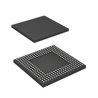
HD6417760BL200AV Renesas Electronics America, HD6417760BL200AV Datasheet - Page 66

HD6417760BL200AV
Manufacturer Part Number
HD6417760BL200AV
Description
SH4 7760, 17 X17 256BGA, LCDC, U
Manufacturer
Renesas Electronics America
Series
SuperH® SH7750r
Datasheet
1.D6417760BP200ADV.pdf
(1418 pages)
Specifications of HD6417760BL200AV
Core Processor
SH-4
Core Size
32-Bit
Speed
200MHz
Connectivity
Audio Codec, CAN, EBI/EMI, FIFO, I²C, MFI, MMC, SCI, Serial Sound, SIM, SPI, USB
Peripherals
DMA, LCD, POR, WDT
Number Of I /o
69
Program Memory Type
ROMless
Ram Size
48K x 8
Voltage - Supply (vcc/vdd)
1.4 V ~ 1.6 V
Data Converters
A/D 4x10b
Oscillator Type
Internal
Operating Temperature
-40°C ~ 85°C
Package / Case
256-BGA
Lead Free Status / RoHS Status
Lead free / RoHS Compliant
Eeprom Size
-
Program Memory Size
-
Available stocks
Company
Part Number
Manufacturer
Quantity
Price
Company:
Part Number:
HD6417760BL200AV
Manufacturer:
Renesas Electronics America
Quantity:
10 000
Part Number:
HD6417760BL200AV
Manufacturer:
RENENAS
Quantity:
20 000
- Current page: 66 of 1418
- Download datasheet (9Mb)
Figure 11.33 Example of SSI DMA Transfer Operation Flow.................................................... 472
Figure 11.34 Forced Termination and Resume Procedures for DMA Audio Transfer................ 474
Figure 11.35 HAC/SSI DMA Transfer Operation Flow Using an Interrupt................................ 475
Figure 11.36 8-Bit Data Transfer for SSI .................................................................................... 477
Figure 11.37 16-Bit Data Transfer for HAC/SSI......................................................................... 477
Figure 11.38 Example of LCDC Data Transfer Flow.................................................................. 478
Figure 11.39 DMA Transfer Flow Shared Memory ↔ Synchronous DRAM ............................ 480
Figure 11.40 Bus Arrangement for Data Alignment ................................................................... 481
Section 12 Clock Pulse Generator (CPG)
Figure 12.1 Block Diagram of CPG .......................................................................................... 488
Figure 12.2 Points for Attention when Using Crystal Resonator .............................................. 501
Figure 12.3 Points for Attention when Using PLL Oscillation Circuit...................................... 502
Section 13 Watchdog Timer (WDT)
Figure 13.1 Block Diagram of WDT......................................................................................... 503
Figure 13.2 Writing to WTCNT and WTCSR........................................................................... 507
Section 14 Power-Down Modes
Figure 14.1 STATUS Output in Power-On Reset ..................................................................... 522
Figure 14.2 STATUS Output in Manual Reset.......................................................................... 523
Figure 14.3 STATUS Output in Sequence of Software Standby → Interrupt........................... 524
Figure 14.4 STATUS Output in Sequence of Software Standby → Power-On Reset............... 524
Figure 14.5 STATUS Output in Sequence of Software Standby → Manual Reset ................... 525
Figure 14.6 STATUS Output in Sequence of Sleep → Interrupt .............................................. 525
Figure 14.7 STATUS Output in Sequence of Sleep → Power-On Reset .................................. 526
Figure 14.8 STATUS Output in Sequence of Sleep → Manual Reset ...................................... 526
Figure 14.9 STATUS Output in Sequence of Deep Sleep → Interrupt ..................................... 527
Figure 14.10 STATUS Output in Sequence of Deep Sleep → Power-On Reset......................... 527
Figure 14.11 STATUS Output in Sequence of Deep Sleep → Manual Reset ............................. 528
Figure 14.12 Hardware Standby Mode Timing (When CA = Low in Normal Operation).......... 529
Figure 14.13 Hardware Standby Mode Timing (When CA = Low in WDT Operation) ............. 530
Figure 14.14 Timing when Power Is Off..................................................................................... 530
Section 15 Timer Unit (TMU)
Figure 15.1 Block Diagram of TMU ......................................................................................... 534
Figure 15.2 Example of Count Operation Setting Procedure .................................................... 541
Figure 15.3 TCNT Auto-Reload Operation............................................................................... 542
Figure 15.4 Count Timing when Operating on Internal Clock .................................................. 542
Figure 15.5 Count Timing when Operating on External Clock................................................. 543
Figure 15.6 Operation Timing when Using Input Capture Function ......................................... 544
Rev. 2.00 Feb. 12, 2010 Page lxiv of lxxxii
REJ09B0554-0200
Related parts for HD6417760BL200AV
Image
Part Number
Description
Manufacturer
Datasheet
Request
R

Part Number:
Description:
KIT STARTER FOR M16C/29
Manufacturer:
Renesas Electronics America
Datasheet:

Part Number:
Description:
KIT STARTER FOR R8C/2D
Manufacturer:
Renesas Electronics America
Datasheet:

Part Number:
Description:
R0K33062P STARTER KIT
Manufacturer:
Renesas Electronics America
Datasheet:

Part Number:
Description:
KIT STARTER FOR R8C/23 E8A
Manufacturer:
Renesas Electronics America
Datasheet:

Part Number:
Description:
KIT STARTER FOR R8C/25
Manufacturer:
Renesas Electronics America
Datasheet:

Part Number:
Description:
KIT STARTER H8S2456 SHARPE DSPLY
Manufacturer:
Renesas Electronics America
Datasheet:

Part Number:
Description:
KIT STARTER FOR R8C38C
Manufacturer:
Renesas Electronics America
Datasheet:

Part Number:
Description:
KIT STARTER FOR R8C35C
Manufacturer:
Renesas Electronics America
Datasheet:

Part Number:
Description:
KIT STARTER FOR R8CL3AC+LCD APPS
Manufacturer:
Renesas Electronics America
Datasheet:

Part Number:
Description:
KIT STARTER FOR RX610
Manufacturer:
Renesas Electronics America
Datasheet:

Part Number:
Description:
KIT STARTER FOR R32C/118
Manufacturer:
Renesas Electronics America
Datasheet:

Part Number:
Description:
KIT DEV RSK-R8C/26-29
Manufacturer:
Renesas Electronics America
Datasheet:

Part Number:
Description:
KIT STARTER FOR SH7124
Manufacturer:
Renesas Electronics America
Datasheet:

Part Number:
Description:
KIT STARTER FOR H8SX/1622
Manufacturer:
Renesas Electronics America
Datasheet:

Part Number:
Description:
KIT DEV FOR SH7203
Manufacturer:
Renesas Electronics America
Datasheet:


