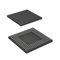
HD6417760BL200AV Renesas Electronics America, HD6417760BL200AV Datasheet - Page 460

HD6417760BL200AV
Manufacturer Part Number
HD6417760BL200AV
Description
SH4 7760, 17 X17 256BGA, LCDC, U
Manufacturer
Renesas Electronics America
Series
SuperH® SH7750r
Datasheet
1.D6417760BP200ADV.pdf
(1418 pages)
Specifications of HD6417760BL200AV
Core Processor
SH-4
Core Size
32-Bit
Speed
200MHz
Connectivity
Audio Codec, CAN, EBI/EMI, FIFO, I²C, MFI, MMC, SCI, Serial Sound, SIM, SPI, USB
Peripherals
DMA, LCD, POR, WDT
Number Of I /o
69
Program Memory Type
ROMless
Ram Size
48K x 8
Voltage - Supply (vcc/vdd)
1.4 V ~ 1.6 V
Data Converters
A/D 4x10b
Oscillator Type
Internal
Operating Temperature
-40°C ~ 85°C
Package / Case
256-BGA
Lead Free Status / RoHS Status
Lead free / RoHS Compliant
Eeprom Size
-
Program Memory Size
-
Available stocks
Company
Part Number
Manufacturer
Quantity
Price
Company:
Part Number:
HD6417760BL200AV
Manufacturer:
Renesas Electronics America
Quantity:
10 000
Part Number:
HD6417760BL200AV
Manufacturer:
RENENAS
Quantity:
20 000
- Current page: 460 of 1418
- Download datasheet (9Mb)
Section 10 Bus State Controller (BSC)
bus. Since signals are driven at the same level by the master and slave transferring the right to
access the bus, output buffer collisions can be avoided.
The right of access to the bus is transferred at the end of bus cycles.
When the bus release request signal (BREQ) is asserted, this LSI releases the bus as soon as the
current bus cycle being executed ends and outputs the bus request acknowledge signal (BACK).
However, the bus is not released during multiple bus cycles generated due to a smaller data bus
width than the access size (such as when performing longword access to 8-bit bus width memory)
or during a 32-byte transfer such as a cache fill or write-back. The bus is also not released between
read and write cycles during execution of a TAS instruction, or between read and write cycles
when DMAC dual address transfer is executed. When BREQ is negated, BACK is negated and use
of the bus is resumed.
When a refresh request is generated, this LSI performs a refresh operation as soon as the current
bus cycle being executed ends. However, refresh operations are deferred during multiple bus
cycles generated due to a smaller data bus width than the access size (such as when performing
longword access to 8-bit bus width memory) and during a 32-byte transfer such as a cache fill or
write-back. The refresh operation is also deferred between read and write cycles during execution
of a TAS instruction, and between read and write cycles when DMAC dual address transfer is
executed. Refresh operations are also deferred in the bus release state.
Since the CPU in this LSI is connected to cache memory by a dedicated peripheral bus, the CPU
can still read from cache memory when the bus is being used by another bus master inside or
outside this LSI. When writing from the CPU, an off-chip write cycle is generated when write-
through has been set for the cache in this LSI, or when an access is made to a cache-off area. This
results in a delay until the bus is returned.
When this LSI wants to take back the bus in response to an internal memory refresh request, it
negates BACK. A device that asserts the off-chip bus release request receives the BACK negation,
and then negates BREQ to release the bus. In this way, the bus is returned to this LSI, and then
processing is performed.
Rev. 2.00 Feb. 12, 2010 Page 376 of 1330
REJ09B0554-0200
Related parts for HD6417760BL200AV
Image
Part Number
Description
Manufacturer
Datasheet
Request
R

Part Number:
Description:
KIT STARTER FOR M16C/29
Manufacturer:
Renesas Electronics America
Datasheet:

Part Number:
Description:
KIT STARTER FOR R8C/2D
Manufacturer:
Renesas Electronics America
Datasheet:

Part Number:
Description:
R0K33062P STARTER KIT
Manufacturer:
Renesas Electronics America
Datasheet:

Part Number:
Description:
KIT STARTER FOR R8C/23 E8A
Manufacturer:
Renesas Electronics America
Datasheet:

Part Number:
Description:
KIT STARTER FOR R8C/25
Manufacturer:
Renesas Electronics America
Datasheet:

Part Number:
Description:
KIT STARTER H8S2456 SHARPE DSPLY
Manufacturer:
Renesas Electronics America
Datasheet:

Part Number:
Description:
KIT STARTER FOR R8C38C
Manufacturer:
Renesas Electronics America
Datasheet:

Part Number:
Description:
KIT STARTER FOR R8C35C
Manufacturer:
Renesas Electronics America
Datasheet:

Part Number:
Description:
KIT STARTER FOR R8CL3AC+LCD APPS
Manufacturer:
Renesas Electronics America
Datasheet:

Part Number:
Description:
KIT STARTER FOR RX610
Manufacturer:
Renesas Electronics America
Datasheet:

Part Number:
Description:
KIT STARTER FOR R32C/118
Manufacturer:
Renesas Electronics America
Datasheet:

Part Number:
Description:
KIT DEV RSK-R8C/26-29
Manufacturer:
Renesas Electronics America
Datasheet:

Part Number:
Description:
KIT STARTER FOR SH7124
Manufacturer:
Renesas Electronics America
Datasheet:

Part Number:
Description:
KIT STARTER FOR H8SX/1622
Manufacturer:
Renesas Electronics America
Datasheet:

Part Number:
Description:
KIT DEV FOR SH7203
Manufacturer:
Renesas Electronics America
Datasheet:


