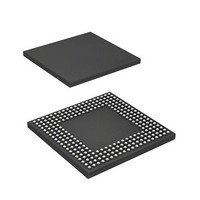
HD6417760BL200AV Renesas Electronics America, HD6417760BL200AV Datasheet - Page 423

HD6417760BL200AV
Manufacturer Part Number
HD6417760BL200AV
Description
SH4 7760, 17 X17 256BGA, LCDC, U
Manufacturer
Renesas Electronics America
Series
SuperH® SH7750r
Datasheet
1.D6417760BP200ADV.pdf
(1418 pages)
Specifications of HD6417760BL200AV
Core Processor
SH-4
Core Size
32-Bit
Speed
200MHz
Connectivity
Audio Codec, CAN, EBI/EMI, FIFO, I²C, MFI, MMC, SCI, Serial Sound, SIM, SPI, USB
Peripherals
DMA, LCD, POR, WDT
Number Of I /o
69
Program Memory Type
ROMless
Ram Size
48K x 8
Voltage - Supply (vcc/vdd)
1.4 V ~ 1.6 V
Data Converters
A/D 4x10b
Oscillator Type
Internal
Operating Temperature
-40°C ~ 85°C
Package / Case
256-BGA
Lead Free Status / RoHS Status
Lead free / RoHS Compliant
Eeprom Size
-
Program Memory Size
-
Available stocks
Company
Part Number
Manufacturer
Quantity
Price
Company:
Part Number:
HD6417760BL200AV
Manufacturer:
Renesas Electronics America
Quantity:
10 000
Part Number:
HD6417760BL200AV
Manufacturer:
RENENAS
Quantity:
20 000
- Current page: 423 of 1418
- Download datasheet (9Mb)
Bus Width
32
32
(c) Relationship between Refresh Requests and Bus Cycle Requests
(10) Power-On Sequence
To use synchronous DRAM, the mode must first be set after power is supplied. To initialize
synchronous DRAM correctly, the bus state controller registers must first be set, and then writing
must be performed to the synchronous DRAM mode register. In the synchronous DRAM mode
register setting, the address signal value at that time is latched by a combination of the RAS, CAS,
and RD/WR signals. If the value to be set is X, the bus state controller operates so that the value X
is written to the synchronous DRAM mode register by performing a write to address H'FF90 0000
+ X for area 2 synchronous DRAM, and to address H'FF94 0000 + X for area 3 synchronous
DRAM. In this operation, the data is ignored, but the mode write is performed as a byte-size
access. To set burst read/burst write, CAS latency 1 to 3, wrap type = sequential, and burst length
4 or 8, which are supported by this LSI, arbitrary data is written in byte-size access to the
following addresses.
If a refresh request is generated during execution of a bus cycle, execution of the refresh is
deferred until the bus cycle is completed. Refresh operations are deferred during multiple bus
cycles generated due to a smaller data bus width than the access size (such as when performing
longword access to 8-bit bus width memory) and during a 32-byte transfer such as a cache fill
or write-back. Refresh operations are also deferred between read and write cycles during
execution of a TAS instruction and between read and write cycles when DMAC dual address
transfer is executed. If a refresh request occurs when the bus has been released by the bus
arbitration function, refresh execution is deferred until the bus is acquired. If a match between
RTCNT and RTCOR occurs while a refresh is waiting to be executed so that a new refresh
request is generated, the previous refresh request is eliminated. In order for refreshing to be
performed correctly, care must be taken to ensure that no bus cycle or bus mastership occurs
that is longer than the refresh interval. When a refresh request is generated, the BACK signal is
negated (driven high). Therefore, correct refreshing can be performed by monitoring the
BACK signal using a bus arbiter or bus master other than this LSI requesting the bus, and
returning the bus to this LSI.
Burst Length CAS Latency
4
8
1
2
3
1
2
3
Area 2
H'FF90 0048
H'FF90 0088
H'FF90 00C8
H'FF90 004C
H'FF90 008C
H'FF90 00CC
Rev. 2.00 Feb. 12, 2010 Page 339 of 1330
Area 3
H'FF94 0048
H'FF94 0088
H'FF94 00C8
H'FF94 004C
H'FF94 008C
H'FF94 00CC
REJ09B0554-0200
Related parts for HD6417760BL200AV
Image
Part Number
Description
Manufacturer
Datasheet
Request
R

Part Number:
Description:
KIT STARTER FOR M16C/29
Manufacturer:
Renesas Electronics America
Datasheet:

Part Number:
Description:
KIT STARTER FOR R8C/2D
Manufacturer:
Renesas Electronics America
Datasheet:

Part Number:
Description:
R0K33062P STARTER KIT
Manufacturer:
Renesas Electronics America
Datasheet:

Part Number:
Description:
KIT STARTER FOR R8C/23 E8A
Manufacturer:
Renesas Electronics America
Datasheet:

Part Number:
Description:
KIT STARTER FOR R8C/25
Manufacturer:
Renesas Electronics America
Datasheet:

Part Number:
Description:
KIT STARTER H8S2456 SHARPE DSPLY
Manufacturer:
Renesas Electronics America
Datasheet:

Part Number:
Description:
KIT STARTER FOR R8C38C
Manufacturer:
Renesas Electronics America
Datasheet:

Part Number:
Description:
KIT STARTER FOR R8C35C
Manufacturer:
Renesas Electronics America
Datasheet:

Part Number:
Description:
KIT STARTER FOR R8CL3AC+LCD APPS
Manufacturer:
Renesas Electronics America
Datasheet:

Part Number:
Description:
KIT STARTER FOR RX610
Manufacturer:
Renesas Electronics America
Datasheet:

Part Number:
Description:
KIT STARTER FOR R32C/118
Manufacturer:
Renesas Electronics America
Datasheet:

Part Number:
Description:
KIT DEV RSK-R8C/26-29
Manufacturer:
Renesas Electronics America
Datasheet:

Part Number:
Description:
KIT STARTER FOR SH7124
Manufacturer:
Renesas Electronics America
Datasheet:

Part Number:
Description:
KIT STARTER FOR H8SX/1622
Manufacturer:
Renesas Electronics America
Datasheet:

Part Number:
Description:
KIT DEV FOR SH7203
Manufacturer:
Renesas Electronics America
Datasheet:


