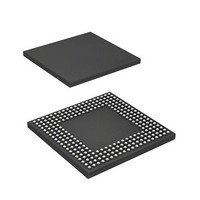
HD6417760BL200AV Renesas Electronics America, HD6417760BL200AV Datasheet - Page 773

HD6417760BL200AV
Manufacturer Part Number
HD6417760BL200AV
Description
SH4 7760, 17 X17 256BGA, LCDC, U
Manufacturer
Renesas Electronics America
Series
SuperH® SH7750r
Datasheet
1.D6417760BP200ADV.pdf
(1418 pages)
Specifications of HD6417760BL200AV
Core Processor
SH-4
Core Size
32-Bit
Speed
200MHz
Connectivity
Audio Codec, CAN, EBI/EMI, FIFO, I²C, MFI, MMC, SCI, Serial Sound, SIM, SPI, USB
Peripherals
DMA, LCD, POR, WDT
Number Of I /o
69
Program Memory Type
ROMless
Ram Size
48K x 8
Voltage - Supply (vcc/vdd)
1.4 V ~ 1.6 V
Data Converters
A/D 4x10b
Oscillator Type
Internal
Operating Temperature
-40°C ~ 85°C
Package / Case
256-BGA
Lead Free Status / RoHS Status
Lead free / RoHS Compliant
Eeprom Size
-
Program Memory Size
-
Available stocks
Company
Part Number
Manufacturer
Quantity
Price
Company:
Part Number:
HD6417760BL200AV
Manufacturer:
Renesas Electronics America
Quantity:
10 000
Part Number:
HD6417760BL200AV
Manufacturer:
RENENAS
Quantity:
20 000
- Current page: 773 of 1418
- Download datasheet (9Mb)
2
Section 19 I
C Bus Interface
(2) MDE and SDE (Single Buffer Mode)
When the slave or master is about to start transmission of data (from the transmit data register)
2
onto the I
C bus, the MDE and SDE status bits may still remain 1. In such case, the SCL line must
be held low until these bits are reset to 0. The MDE and SDE bits being set to 1 indicate that the
2
data has already been transmitted from the transmit data register onto the I
C bus.
To write data into the transmit data register that is ready for the next transmission, the software
must clear MDE and SDE to 0. However, this is not required for the first byte transmission onto
the bus.
(3) MAL
When the master has lost arbitration, the MAL bit in the master status register is set to 1 and the
MIE bit in the master control register is reset to 0. At this point, the master mode is disabled and
2
the I
C bus interface is set to operate in the slave mode. When master operation is restarted, data
transfer from the master begins after the MAL bit has been cleared to 0.
(4) SAR
2
The SAR status bit is set to 1 when the slave has recognized its address output to the I
C bus. At
this point, the slave interface drives the SCL line to be low until the SAR status bit is reset to 0.
This is particularly important when a slave transmit is about to take place on the bus. When the
slave transmits the data from the transmit data register, the software responds to the SAR status by
writing the required data into the transmit data register and resetting the SAR status bit to 0. This
allows the slave interface to carry on access.
When the slave is about to receive data, the software may not have completed reading of data
loaded by the previous access from the receive data register. The problem is that the new access
may overwrite the valid data still held in the receive data register. However, this can be avoided by
using the SAR status bit. The software should reset the SAR bit to 0 (if it is set to 1) only after
completing a read from the receive data register. Then the receive data register will not be
overwritten.
(5) Writing to ICTXD and the TDFE Flag (FIFO Buffer Mode)
The TDFE flag of ICFSR is set to 1 when the byte count in ICTXD is equal to or smaller than the
transmit trigger byte count by TTRG1 and TTRG0 bits of ICFCR. After TDFE is set, the transmit
data can be written for the number of empty bytes in ICTXD. This allows efficient continuous
transmission. When the byte count in ICTXD is below the transmit trigger count, the TDFE flag is
automatically set to 1 even if the flag is cleared to 0. Accordingly, clear the TDFE flag to 0 only
Rev. 2.00 Feb. 12, 2010 Page 689 of 1330
REJ09B0554-0200
Related parts for HD6417760BL200AV
Image
Part Number
Description
Manufacturer
Datasheet
Request
R

Part Number:
Description:
KIT STARTER FOR M16C/29
Manufacturer:
Renesas Electronics America
Datasheet:

Part Number:
Description:
KIT STARTER FOR R8C/2D
Manufacturer:
Renesas Electronics America
Datasheet:

Part Number:
Description:
R0K33062P STARTER KIT
Manufacturer:
Renesas Electronics America
Datasheet:

Part Number:
Description:
KIT STARTER FOR R8C/23 E8A
Manufacturer:
Renesas Electronics America
Datasheet:

Part Number:
Description:
KIT STARTER FOR R8C/25
Manufacturer:
Renesas Electronics America
Datasheet:

Part Number:
Description:
KIT STARTER H8S2456 SHARPE DSPLY
Manufacturer:
Renesas Electronics America
Datasheet:

Part Number:
Description:
KIT STARTER FOR R8C38C
Manufacturer:
Renesas Electronics America
Datasheet:

Part Number:
Description:
KIT STARTER FOR R8C35C
Manufacturer:
Renesas Electronics America
Datasheet:

Part Number:
Description:
KIT STARTER FOR R8CL3AC+LCD APPS
Manufacturer:
Renesas Electronics America
Datasheet:

Part Number:
Description:
KIT STARTER FOR RX610
Manufacturer:
Renesas Electronics America
Datasheet:

Part Number:
Description:
KIT STARTER FOR R32C/118
Manufacturer:
Renesas Electronics America
Datasheet:

Part Number:
Description:
KIT DEV RSK-R8C/26-29
Manufacturer:
Renesas Electronics America
Datasheet:

Part Number:
Description:
KIT STARTER FOR SH7124
Manufacturer:
Renesas Electronics America
Datasheet:

Part Number:
Description:
KIT STARTER FOR H8SX/1622
Manufacturer:
Renesas Electronics America
Datasheet:

Part Number:
Description:
KIT DEV FOR SH7203
Manufacturer:
Renesas Electronics America
Datasheet:


