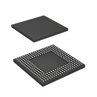
HD6417760BL200AV Renesas Electronics America, HD6417760BL200AV Datasheet - Page 73

HD6417760BL200AV
Manufacturer Part Number
HD6417760BL200AV
Description
SH4 7760, 17 X17 256BGA, LCDC, U
Manufacturer
Renesas Electronics America
Series
SuperH® SH7750r
Datasheet
1.D6417760BP200ADV.pdf
(1418 pages)
Specifications of HD6417760BL200AV
Core Processor
SH-4
Core Size
32-Bit
Speed
200MHz
Connectivity
Audio Codec, CAN, EBI/EMI, FIFO, I²C, MFI, MMC, SCI, Serial Sound, SIM, SPI, USB
Peripherals
DMA, LCD, POR, WDT
Number Of I /o
69
Program Memory Type
ROMless
Ram Size
48K x 8
Voltage - Supply (vcc/vdd)
1.4 V ~ 1.6 V
Data Converters
A/D 4x10b
Oscillator Type
Internal
Operating Temperature
-40°C ~ 85°C
Package / Case
256-BGA
Lead Free Status / RoHS Status
Lead free / RoHS Compliant
Eeprom Size
-
Program Memory Size
-
Available stocks
Company
Part Number
Manufacturer
Quantity
Price
Company:
Part Number:
HD6417760BL200AV
Manufacturer:
Renesas Electronics America
Quantity:
10 000
Part Number:
HD6417760BL200AV
Manufacturer:
RENENAS
Quantity:
20 000
- Current page: 73 of 1418
- Download datasheet (9Mb)
Figure 33.12 PLL Synchronization Settling Time in Case of RESET, MRESET or
Figure 33.13 PLL Synchronization Settling Time in Case of IRL Interrupt.............................. 1235
Figure 33.14 MD pins Setup/Hold Timing ................................................................................ 1236
Figure 33.15 Control Signal Timing.......................................................................................... 1237
Figure 33.16 (1) Pin Drive Timing for Reset or Sleep Mode .................................................. 1237
Figure 33.16 (2) Pin Drive Timing for Software Standby Mode ............................................. 1238
Figure 33.17 SRAM Bus Cycle: Basic Bus Cycle (No Wait).................................................... 1240
Figure 33.18 SRAM Bus Cycle: Basic Bus Cycle (One Internal Wait) .................................... 1241
Figure 33.19 SRAM Bus Cycle: Basic Bus Cycle (One Internal Wait + One External
Figure 33.20 SRAM Bus Cycle: Basic Bus Cycle (No Wait, Address Setup/Hold Time
Figure 33.21 Burst ROM Bus Cycle (No Wait) ........................................................................ 1244
Figure 33.22 Burst ROM Bus Cycle (1st Data: One Internal Wait + One External Wait ;
Figure 33.23 Burst ROM Bus Cycle (No Wait, Address Setup/Hold Time Insertion, AnS = 1,
Figure 33.24 Burst ROM Bus Cycle (One Internal Wait + One External Wait) ....................... 1247
Figure 33.25 Synchronous DRAN Auto-Precharge Read Bus Cycle: Single (RCD[1:0] = 01,
Figure 33.26 Synchronous DRAM Auto-Precharge Read Bus Cycle: Burst (RCD[1:0] = 01,
Figure 33.27 Synchronous DRAM Normal Read Bus Cycle: ACT + READ Commands,
Figure 33.28 Synchronous DRAM Normal Read Bus Cycle: PRE + ACT + READ Commands,
Figure 33.29 Synchronous DRAM Normal Read Bus Cycle: READ Command, Burst (CAS
Figure 33.30 Synchronous DRAM Auto-Precharge Write Bus Cycle: Single (RCD[1:0] = 01,
Figure 33.31 Synchronous DRAM Auto-Precharge Write Bus Cycle: Burst (RCD[1:0] = 01,
Figure 33.32 Synchronous DRAM Normal Write Bus Cycle: ACT+WRITE Commands,
Figure 33.33 Synchronous DRAM Normal Write Bus Cycle: PRE+ACT+WRITE Commands,
Figure 33.34 Synchronous DRAM Normal Write Bus Cycle: WRITE Command, Burst
Figure 33.35 Synchronous DRAM Bus Cycle: Precharge Command (TPC[2:0] = 001) .......... 1258
Figure 33.36 Synchronous DRAM Bus Cycle: Auto-Refresh (TRAS = 1, TRC[2:0] = 001) ... 1259
Figure 33.37 Synchronous DRAM Bus Cycle: Self-Refresh (TRC[2:0] = 001) ....................... 1260
NMI Interrupt ....................................................................................................... 1235
Wait)..................................................................................................................... 1242
Insertion, AnS = 1, AnH = 1) ............................................................................... 1243
2nd/3rd/4th Data: One Internal Wait)................................................................... 1245
AnH = 1) .............................................................................................................. 1246
CAS Latency = 3, TPC[2:0] = 011)...................................................................... 1248
CAS Latency = 3, TPC[2:0] = 011)...................................................................... 1249
Burst (RCD[1:0] = 01, CAS Latency = 3)............................................................ 1250
Burst (RCD[1:0] = 01, TPC[2:0] = 001, CAS Latency = 3)................................. 1251
Latency = 3) ......................................................................................................... 1252
TPC[2:0] = 001, TRWL[2:0] = 010) .................................................................... 1253
TPC[2:0] = 001, TRWL[2:0] = 010) .................................................................... 1254
Burst (RCD[1:0] = 01, TRWL[2:0] = 010) .......................................................... 1255
Burst (RCD[1:0] = 01, TPC[2:0] = 001, TRWL[2:0] = 010) ............................... 1256
(TRWL[2:0] = 010) .............................................................................................. 1257
Rev. 2.00 Feb. 12, 2010 Page lxxi of lxxxii
REJ09B0554-0200
Related parts for HD6417760BL200AV
Image
Part Number
Description
Manufacturer
Datasheet
Request
R

Part Number:
Description:
KIT STARTER FOR M16C/29
Manufacturer:
Renesas Electronics America
Datasheet:

Part Number:
Description:
KIT STARTER FOR R8C/2D
Manufacturer:
Renesas Electronics America
Datasheet:

Part Number:
Description:
R0K33062P STARTER KIT
Manufacturer:
Renesas Electronics America
Datasheet:

Part Number:
Description:
KIT STARTER FOR R8C/23 E8A
Manufacturer:
Renesas Electronics America
Datasheet:

Part Number:
Description:
KIT STARTER FOR R8C/25
Manufacturer:
Renesas Electronics America
Datasheet:

Part Number:
Description:
KIT STARTER H8S2456 SHARPE DSPLY
Manufacturer:
Renesas Electronics America
Datasheet:

Part Number:
Description:
KIT STARTER FOR R8C38C
Manufacturer:
Renesas Electronics America
Datasheet:

Part Number:
Description:
KIT STARTER FOR R8C35C
Manufacturer:
Renesas Electronics America
Datasheet:

Part Number:
Description:
KIT STARTER FOR R8CL3AC+LCD APPS
Manufacturer:
Renesas Electronics America
Datasheet:

Part Number:
Description:
KIT STARTER FOR RX610
Manufacturer:
Renesas Electronics America
Datasheet:

Part Number:
Description:
KIT STARTER FOR R32C/118
Manufacturer:
Renesas Electronics America
Datasheet:

Part Number:
Description:
KIT DEV RSK-R8C/26-29
Manufacturer:
Renesas Electronics America
Datasheet:

Part Number:
Description:
KIT STARTER FOR SH7124
Manufacturer:
Renesas Electronics America
Datasheet:

Part Number:
Description:
KIT STARTER FOR H8SX/1622
Manufacturer:
Renesas Electronics America
Datasheet:

Part Number:
Description:
KIT DEV FOR SH7203
Manufacturer:
Renesas Electronics America
Datasheet:


