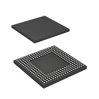
HD6417760BL200AV Renesas Electronics America, HD6417760BL200AV Datasheet - Page 335

HD6417760BL200AV
Manufacturer Part Number
HD6417760BL200AV
Description
SH4 7760, 17 X17 256BGA, LCDC, U
Manufacturer
Renesas Electronics America
Series
SuperH® SH7750r
Datasheet
1.D6417760BP200ADV.pdf
(1418 pages)
Specifications of HD6417760BL200AV
Core Processor
SH-4
Core Size
32-Bit
Speed
200MHz
Connectivity
Audio Codec, CAN, EBI/EMI, FIFO, I²C, MFI, MMC, SCI, Serial Sound, SIM, SPI, USB
Peripherals
DMA, LCD, POR, WDT
Number Of I /o
69
Program Memory Type
ROMless
Ram Size
48K x 8
Voltage - Supply (vcc/vdd)
1.4 V ~ 1.6 V
Data Converters
A/D 4x10b
Oscillator Type
Internal
Operating Temperature
-40°C ~ 85°C
Package / Case
256-BGA
Lead Free Status / RoHS Status
Lead free / RoHS Compliant
Eeprom Size
-
Program Memory Size
-
Available stocks
Company
Part Number
Manufacturer
Quantity
Price
Company:
Part Number:
HD6417760BL200AV
Manufacturer:
Renesas Electronics America
Quantity:
10 000
Part Number:
HD6417760BL200AV
Manufacturer:
RENENAS
Quantity:
20 000
- Current page: 335 of 1418
- Download datasheet (9Mb)
Name
Data enable 2
Data enable 3
Ready
Area 0 MPX
interface setting/
16-bit I/O
Clock enable
Bus release
request
Bus request
acknowledge
Area 0 bus
width/PCMCIA
card select
Endian switchover MD5
Note:
10.3
(1) Space Divisions
The architecture of this LSI provides a 32-bit virtual address space. The virtual address space is
divided into five areas according to the upper address value. Off-chip memory space comprises a
29-bit address space, divided into eight areas.
The virtual address space can be allocated to any off-chip address by means of the memory
management unit (MMU). Details are given in section 6, Memory Management Unit (MMU).
This section describes the areas into which the off-chip address space is divided.
* The input/output switching is specified by the A56PCM bit in bus control register 1
Overview of Areas
(BCR1).
Signals
WE2/
DQM2/
ICIORD
WE3/
DQM3/
ICIOWR
RDY
MD6/IOIS16
CKE
BREQ
BACK
MD3/CE2A*
MD4/CE2B*
I/O
Output When setting PCMCIA interface: ICIORD signal
Output When setting PCMCIA interface: ICIOWR signal
Input
Input
Output Synchronous DRAM clock enable control signal
Input
Output Bus request acknowledge signal
Input/
Output
Input
Description
When setting SRAM interface: write strobe signal for
D23 to D16
When setting synchronous DRAM interface:
selection signal for D23 to D16
When setting SRAM interface: write strobe signal for
D31 to D24
When setting synchronous DRAM interface:
selection signal for D31 to D24
Wait-cycle request signal
At power-on reset: Designates area 0 bus as MPX
interface (1: SRAM, 0: MPX)
When setting PCMCIA interface: 16-bit I/O
designation signal. Valid only in little-endian mode.
Bus release request signal
At power-on reset: area 0 bus width specification
signal
When using PCMCIA: CE2A, CE2B
Endian setting at a power-on reset
Rev. 2.00 Feb. 12, 2010 Page 251 of 1330
REJ09B0554-0200
Related parts for HD6417760BL200AV
Image
Part Number
Description
Manufacturer
Datasheet
Request
R

Part Number:
Description:
KIT STARTER FOR M16C/29
Manufacturer:
Renesas Electronics America
Datasheet:

Part Number:
Description:
KIT STARTER FOR R8C/2D
Manufacturer:
Renesas Electronics America
Datasheet:

Part Number:
Description:
R0K33062P STARTER KIT
Manufacturer:
Renesas Electronics America
Datasheet:

Part Number:
Description:
KIT STARTER FOR R8C/23 E8A
Manufacturer:
Renesas Electronics America
Datasheet:

Part Number:
Description:
KIT STARTER FOR R8C/25
Manufacturer:
Renesas Electronics America
Datasheet:

Part Number:
Description:
KIT STARTER H8S2456 SHARPE DSPLY
Manufacturer:
Renesas Electronics America
Datasheet:

Part Number:
Description:
KIT STARTER FOR R8C38C
Manufacturer:
Renesas Electronics America
Datasheet:

Part Number:
Description:
KIT STARTER FOR R8C35C
Manufacturer:
Renesas Electronics America
Datasheet:

Part Number:
Description:
KIT STARTER FOR R8CL3AC+LCD APPS
Manufacturer:
Renesas Electronics America
Datasheet:

Part Number:
Description:
KIT STARTER FOR RX610
Manufacturer:
Renesas Electronics America
Datasheet:

Part Number:
Description:
KIT STARTER FOR R32C/118
Manufacturer:
Renesas Electronics America
Datasheet:

Part Number:
Description:
KIT DEV RSK-R8C/26-29
Manufacturer:
Renesas Electronics America
Datasheet:

Part Number:
Description:
KIT STARTER FOR SH7124
Manufacturer:
Renesas Electronics America
Datasheet:

Part Number:
Description:
KIT STARTER FOR H8SX/1622
Manufacturer:
Renesas Electronics America
Datasheet:

Part Number:
Description:
KIT DEV FOR SH7203
Manufacturer:
Renesas Electronics America
Datasheet:


