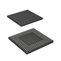
HD6417760BL200AV Renesas Electronics America, HD6417760BL200AV Datasheet - Page 71

HD6417760BL200AV
Manufacturer Part Number
HD6417760BL200AV
Description
SH4 7760, 17 X17 256BGA, LCDC, U
Manufacturer
Renesas Electronics America
Series
SuperH® SH7750r
Datasheet
1.D6417760BP200ADV.pdf
(1418 pages)
Specifications of HD6417760BL200AV
Core Processor
SH-4
Core Size
32-Bit
Speed
200MHz
Connectivity
Audio Codec, CAN, EBI/EMI, FIFO, I²C, MFI, MMC, SCI, Serial Sound, SIM, SPI, USB
Peripherals
DMA, LCD, POR, WDT
Number Of I /o
69
Program Memory Type
ROMless
Ram Size
48K x 8
Voltage - Supply (vcc/vdd)
1.4 V ~ 1.6 V
Data Converters
A/D 4x10b
Oscillator Type
Internal
Operating Temperature
-40°C ~ 85°C
Package / Case
256-BGA
Lead Free Status / RoHS Status
Lead free / RoHS Compliant
Eeprom Size
-
Program Memory Size
-
Available stocks
Company
Part Number
Manufacturer
Quantity
Price
Company:
Part Number:
HD6417760BL200AV
Manufacturer:
Renesas Electronics America
Quantity:
10 000
Part Number:
HD6417760BL200AV
Manufacturer:
RENENAS
Quantity:
20 000
- Current page: 71 of 1418
- Download datasheet (9Mb)
Figure 26.18 Example of Command Sequence for Commands with Write Data
Figure 26.19 Example of Operational Flow for Commands with Write Data
Figure 26.20 Example of Operational Flow for Commands with Write Data
Figure 26.21 Example of Operational Flow for Commands with Write Data
Figure 26.22 Example of Read Sequence Flow...........................................................................992
Figure 26.23 Example of Write Sequence Flow ..........................................................................993
Figure 26.24 Timing of Receiving the Command Response and Data........................................995
Section 27 Multifunctional Interface (MFI)
Figure 27.1 MFI block diagram.................................................................................................998
Figure 27.2 Differences in EDN Bit Settings .......................................................................... 1005
Figure 27.3 Example of MFI Connections .............................................................................. 1013
Figure 27.4 Basic Timing for the MFI 68-Series Interface...................................................... 1014
Figure 27.5 Basic Timing of the MFI 80-Series Interface....................................................... 1015
Figure 27.6 Writing to MFIIDX and Reading from MFIGSR................................................. 1016
Figure 27.7 MFI Register Settings........................................................................................... 1016
Figure 27.8 Continuous Data Writing to MFRAM
Figure 27.9 Continuous Data Reading from MFRAM
Section 28 User Debug Interface (H-UDI)
Figure 28.1 H-UDI Block Diagram ......................................................................................... 1020
Figure 28.2 TAP Controller State Transitions ......................................................................... 1036
Figure 28.3 H-UDI Reset......................................................................................................... 1037
Section 29 A/D Converter (ADC)
Figure 29.1 A/D Converter Block Diagram............................................................................. 1040
Figure 29.2 Example of A/D Converter Operation (Single Mode, Channel 1 Selected) ......... 1048
Figure 29.3 Example of A/D Converter Operation (Multi Mode, Three Channels AN0 to
Figure 29.4 Example of A/D Converter Operation (Scan Mode, Three Channels AN0 to
Figure 29.5 Timing for Data Write when Four Channels Are Selected in Multi Mode .......... 1053
Figure 29.6 External Trigger Input Timing ............................................................................. 1055
Figure 29.7 Definitions of A/D Conversion Accuracy ............................................................ 1057
Figure 29.8 Example of Analog Input Pin Protection Circuit.................................................. 1058
Figure 29.9 Analog Input Pin Equivalent Circuit .................................................................... 1058
(Stream Transfer) ...................................................................................................986
(Single Block Transfer) ..........................................................................................987
(Multiblock Transfer) .............................................................................................988
(Stream Transfer) ...................................................................................................989
(8-Bit Bus Width, MFISCR.SCRMD2 = 0) ......................................................... 1017
(8-Bit Bus Width, MFISCR.SCRMD2 = 0) ......................................................... 1017
AN2 Selected) ...................................................................................................... 1050
AN2 Selected) ...................................................................................................... 1052
Rev. 2.00 Feb. 12, 2010 Page lxix of lxxxii
REJ09B0554-0200
Related parts for HD6417760BL200AV
Image
Part Number
Description
Manufacturer
Datasheet
Request
R

Part Number:
Description:
KIT STARTER FOR M16C/29
Manufacturer:
Renesas Electronics America
Datasheet:

Part Number:
Description:
KIT STARTER FOR R8C/2D
Manufacturer:
Renesas Electronics America
Datasheet:

Part Number:
Description:
R0K33062P STARTER KIT
Manufacturer:
Renesas Electronics America
Datasheet:

Part Number:
Description:
KIT STARTER FOR R8C/23 E8A
Manufacturer:
Renesas Electronics America
Datasheet:

Part Number:
Description:
KIT STARTER FOR R8C/25
Manufacturer:
Renesas Electronics America
Datasheet:

Part Number:
Description:
KIT STARTER H8S2456 SHARPE DSPLY
Manufacturer:
Renesas Electronics America
Datasheet:

Part Number:
Description:
KIT STARTER FOR R8C38C
Manufacturer:
Renesas Electronics America
Datasheet:

Part Number:
Description:
KIT STARTER FOR R8C35C
Manufacturer:
Renesas Electronics America
Datasheet:

Part Number:
Description:
KIT STARTER FOR R8CL3AC+LCD APPS
Manufacturer:
Renesas Electronics America
Datasheet:

Part Number:
Description:
KIT STARTER FOR RX610
Manufacturer:
Renesas Electronics America
Datasheet:

Part Number:
Description:
KIT STARTER FOR R32C/118
Manufacturer:
Renesas Electronics America
Datasheet:

Part Number:
Description:
KIT DEV RSK-R8C/26-29
Manufacturer:
Renesas Electronics America
Datasheet:

Part Number:
Description:
KIT STARTER FOR SH7124
Manufacturer:
Renesas Electronics America
Datasheet:

Part Number:
Description:
KIT STARTER FOR H8SX/1622
Manufacturer:
Renesas Electronics America
Datasheet:

Part Number:
Description:
KIT DEV FOR SH7203
Manufacturer:
Renesas Electronics America
Datasheet:


