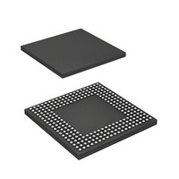
HD6417760BL200AV Renesas Electronics America, HD6417760BL200AV Datasheet - Page 1143

HD6417760BL200AV
Manufacturer Part Number
HD6417760BL200AV
Description
SH4 7760, 17 X17 256BGA, LCDC, U
Manufacturer
Renesas Electronics America
Series
SuperH® SH7750r
Datasheet
1.D6417760BP200ADV.pdf
(1418 pages)
Specifications of HD6417760BL200AV
Core Processor
SH-4
Core Size
32-Bit
Speed
200MHz
Connectivity
Audio Codec, CAN, EBI/EMI, FIFO, I²C, MFI, MMC, SCI, Serial Sound, SIM, SPI, USB
Peripherals
DMA, LCD, POR, WDT
Number Of I /o
69
Program Memory Type
ROMless
Ram Size
48K x 8
Voltage - Supply (vcc/vdd)
1.4 V ~ 1.6 V
Data Converters
A/D 4x10b
Oscillator Type
Internal
Operating Temperature
-40°C ~ 85°C
Package / Case
256-BGA
Lead Free Status / RoHS Status
Lead free / RoHS Compliant
Eeprom Size
-
Program Memory Size
-
Available stocks
Company
Part Number
Manufacturer
Quantity
Price
Company:
Part Number:
HD6417760BL200AV
Manufacturer:
Renesas Electronics America
Quantity:
10 000
Part Number:
HD6417760BL200AV
Manufacturer:
RENENAS
Quantity:
20 000
- Current page: 1143 of 1418
- Download datasheet (9Mb)
29.7.3
Four types of divided clocks can be used as the clock for A/D conversion. Since the internal circuit
configuration affects the limits of the interface between the analog and digital sections, be sure to
see table 29.5 when setting the input clock and clock division ratio.
Table 29.5 Relationship between Clock Division Ratio and Usable Input Clock Frequency
29.7.4
Before entering hardware standby, module standby, or software standby modes, check that A/D
conversion is not in progress, that is, the ADF bit is 1, or in multi mode or scan mode, clear the
ADST bit to 0 to stop A/D conversion. Note that A/D conversion does not stop immediately. If
module standby or software standby mode is entered without confirming that A/D conversion is
stopped, correct AD converter operation is not guaranteed.
In hardware standby, module standby, or software standby mode, all AD converter registers are
initialized.
29.7.5
(1) Condition
When DMAC selection bit (DMASL) of ADCSR is set to 1, the value of ADC register read by
CPU is unknown. Then, ADC registers can't be read during ADC DMA transmission. But writing
register is possible. And while ADC execute DMA transmission, if CPU read MFI register, the
value may not be correct. Furthermore, DMA transmitted value of ADC also may not be correct.
(2) Workaround
Please apply one of following 1) or 2) workarounds.
1) Do not read ADC registers by CPU during ADCSR.DMASL = 1.
2) Use ADCSR.DMASL = 0.
Clock Division Ratio
Pck/4
Pck/8
Pck/16
Pck/32
Pck and Clock Division Ratio Settings
Notes on Standby Modes
Notice of the DMA transmission of A/D converter
Input Clock
18 MHz or lower
34 MHz or lower
34 MHz or lower
34 MHz or lower
Rev. 2.00 Feb. 12, 2010 Page 1059 of 1330
REJ09B0554-0200
Related parts for HD6417760BL200AV
Image
Part Number
Description
Manufacturer
Datasheet
Request
R

Part Number:
Description:
KIT STARTER FOR M16C/29
Manufacturer:
Renesas Electronics America
Datasheet:

Part Number:
Description:
KIT STARTER FOR R8C/2D
Manufacturer:
Renesas Electronics America
Datasheet:

Part Number:
Description:
R0K33062P STARTER KIT
Manufacturer:
Renesas Electronics America
Datasheet:

Part Number:
Description:
KIT STARTER FOR R8C/23 E8A
Manufacturer:
Renesas Electronics America
Datasheet:

Part Number:
Description:
KIT STARTER FOR R8C/25
Manufacturer:
Renesas Electronics America
Datasheet:

Part Number:
Description:
KIT STARTER H8S2456 SHARPE DSPLY
Manufacturer:
Renesas Electronics America
Datasheet:

Part Number:
Description:
KIT STARTER FOR R8C38C
Manufacturer:
Renesas Electronics America
Datasheet:

Part Number:
Description:
KIT STARTER FOR R8C35C
Manufacturer:
Renesas Electronics America
Datasheet:

Part Number:
Description:
KIT STARTER FOR R8CL3AC+LCD APPS
Manufacturer:
Renesas Electronics America
Datasheet:

Part Number:
Description:
KIT STARTER FOR RX610
Manufacturer:
Renesas Electronics America
Datasheet:

Part Number:
Description:
KIT STARTER FOR R32C/118
Manufacturer:
Renesas Electronics America
Datasheet:

Part Number:
Description:
KIT DEV RSK-R8C/26-29
Manufacturer:
Renesas Electronics America
Datasheet:

Part Number:
Description:
KIT STARTER FOR SH7124
Manufacturer:
Renesas Electronics America
Datasheet:

Part Number:
Description:
KIT STARTER FOR H8SX/1622
Manufacturer:
Renesas Electronics America
Datasheet:

Part Number:
Description:
KIT DEV FOR SH7203
Manufacturer:
Renesas Electronics America
Datasheet:


