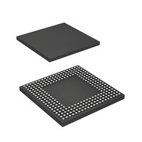
HD6417760BL200AV Renesas Electronics America, HD6417760BL200AV Datasheet - Page 731

HD6417760BL200AV
Manufacturer Part Number
HD6417760BL200AV
Description
SH4 7760, 17 X17 256BGA, LCDC, U
Manufacturer
Renesas Electronics America
Series
SuperH® SH7750r
Datasheet
1.D6417760BP200ADV.pdf
(1418 pages)
Specifications of HD6417760BL200AV
Core Processor
SH-4
Core Size
32-Bit
Speed
200MHz
Connectivity
Audio Codec, CAN, EBI/EMI, FIFO, I²C, MFI, MMC, SCI, Serial Sound, SIM, SPI, USB
Peripherals
DMA, LCD, POR, WDT
Number Of I /o
69
Program Memory Type
ROMless
Ram Size
48K x 8
Voltage - Supply (vcc/vdd)
1.4 V ~ 1.6 V
Data Converters
A/D 4x10b
Oscillator Type
Internal
Operating Temperature
-40°C ~ 85°C
Package / Case
256-BGA
Lead Free Status / RoHS Status
Lead free / RoHS Compliant
Eeprom Size
-
Program Memory Size
-
Available stocks
Company
Part Number
Manufacturer
Quantity
Price
Company:
Part Number:
HD6417760BL200AV
Manufacturer:
Renesas Electronics America
Quantity:
10 000
Part Number:
HD6417760BL200AV
Manufacturer:
RENENAS
Quantity:
20 000
- Current page: 731 of 1418
- Download datasheet (9Mb)
18.3.13 Sampling Register (SISMPL)
SISMPL is a 16-bit readable/writable register that sets the number of serial clock cycles per etu.
Initial value:
Legend: etu: Elementary time unit
18.4
The main functions of the SMI are as follows.
1. One frame consists of eight data bits and one parity bit.
2. The transmitter inserts the guardtime, specified by SIGRD and the LCB and PB bits in
3. When detecting a parity error, the receiver in T = 0 mode outputs low level for 1 etu as an error
4. When sampling an error signal, the transmitter in T = 0 mode automatically repeats the
5. Only asynchronous communication functions are supported; there is no clock-synchronized
18.4.1
Figure 18.2 shows the data format used by the smart card interface. The smart card interface
performs a parity check for each frame during reception.
When detecting a parity error, the receiver in T = 0 mode returns an error signal to the transmitter,
requesting data repetition. The transmitter samples error signals and repeats the disputed data.
Bit
15 to 11
10 to 0
SISCMR, between the end of each parity bit and the beginning of the next frame.
signal, after 10.5 etu has passed since the start bit was received.
disputed data after a delay of at least 2 etu.
communication function.
R/W:
Bit:
Operation
Data Format
15
R
-
0
SISMPL
Bit
Name
⎯
10 to 0
14
R
0
-
13
R
0
-
Initial
Value
All 0
H'173
12
R
0
-
11
R
0
-
R/W
R
R/W
SISM
PL10
R/W
10
0
SISM
Description
Reserved
These bits are always read as 0. The write value
should always be 0.
Setting for the number of serial clock cycles per etu
The number of serial clock cycles per etu is (SISMPL
value + 1). The value written to SISMPL should
always be H'0007 or greater.
R/W
PL9
9
0
SISM
PL8
R/W
8
1
SISM
PL7
R/W
7
0
Rev. 2.00 Feb. 12, 2010 Page 647 of 1330
SISM
R/W
PL6
6
1
SISM
PL5
R/W
5
1
SISM
R/W
PL4
4
1
SISM
R/W
PL3
3
0
REJ09B0554-0200
SISM
PL2
R/W
2
0
SISM
R/W
PL1
1
1
SISM
PL0
R/W
0
1
Related parts for HD6417760BL200AV
Image
Part Number
Description
Manufacturer
Datasheet
Request
R

Part Number:
Description:
KIT STARTER FOR M16C/29
Manufacturer:
Renesas Electronics America
Datasheet:

Part Number:
Description:
KIT STARTER FOR R8C/2D
Manufacturer:
Renesas Electronics America
Datasheet:

Part Number:
Description:
R0K33062P STARTER KIT
Manufacturer:
Renesas Electronics America
Datasheet:

Part Number:
Description:
KIT STARTER FOR R8C/23 E8A
Manufacturer:
Renesas Electronics America
Datasheet:

Part Number:
Description:
KIT STARTER FOR R8C/25
Manufacturer:
Renesas Electronics America
Datasheet:

Part Number:
Description:
KIT STARTER H8S2456 SHARPE DSPLY
Manufacturer:
Renesas Electronics America
Datasheet:

Part Number:
Description:
KIT STARTER FOR R8C38C
Manufacturer:
Renesas Electronics America
Datasheet:

Part Number:
Description:
KIT STARTER FOR R8C35C
Manufacturer:
Renesas Electronics America
Datasheet:

Part Number:
Description:
KIT STARTER FOR R8CL3AC+LCD APPS
Manufacturer:
Renesas Electronics America
Datasheet:

Part Number:
Description:
KIT STARTER FOR RX610
Manufacturer:
Renesas Electronics America
Datasheet:

Part Number:
Description:
KIT STARTER FOR R32C/118
Manufacturer:
Renesas Electronics America
Datasheet:

Part Number:
Description:
KIT DEV RSK-R8C/26-29
Manufacturer:
Renesas Electronics America
Datasheet:

Part Number:
Description:
KIT STARTER FOR SH7124
Manufacturer:
Renesas Electronics America
Datasheet:

Part Number:
Description:
KIT STARTER FOR H8SX/1622
Manufacturer:
Renesas Electronics America
Datasheet:

Part Number:
Description:
KIT DEV FOR SH7203
Manufacturer:
Renesas Electronics America
Datasheet:


